ZHCSDC4 February 2015 UCC28730
PRODUCTION DATA.
- 1 特性
- 2 应用
- 3 说明
- 4 修订历史记录
- 5 Pin Configuration and Functions
- 6 Specifications
- 7 Detailed Description
-
8 Application and Implementation
- 8.1 Application Information
- 8.2
Typical Application
- 8.2.1 Design Requirements
- 8.2.2
Detailed Design Procedure
- 8.2.2.1 Stand-By Power Estimate
- 8.2.2.2 Input Bulk Capacitance and Minimum Bulk Voltage
- 8.2.2.3 Transformer Turns Ratio, Inductance, Primary-Peak Current
- 8.2.2.4 Transformer Parameter Verification
- 8.2.2.5 Output Capacitance
- 8.2.2.6 VDD Capacitance, CVDD
- 8.2.2.7 VS Resistor Divider, Line Compensation, and Cable Compensation
- 8.2.2.8 VS Wake-Up Detection
- 8.2.3 Application Curves
- 8.3 Do's and Don'ts
- 9 Power Supply Recommendations
- 10Layout
- 11器件和文档支持
- 12机械封装和可订购信息
7 Detailed Description
7.1 Overview
The UCC28730 is an isolated-flyback power supply controller which provides accurate voltage and constant current regulation using primary-side winding sensing, eliminating the need for opto-coupler feedback circuits. The controller operates in discontinuous conduction mode with valley switching to minimize switching losses. The modulation scheme is a combination of frequency modulation and primary peak-current modulation to provide high conversion efficiency across the load range. The control law provides a wide dynamic operating range of output power which facilitates the achievement of <5-mW stand-by power.
During low-power operating levels the device has power management features to reduce the device operating current at switching frequencies less than 28 kHz. The UCC28730 includes features in the pulse-width modulator to reduce the EMI peak energy at the fundamental switching frequency and its harmonics. Accurate voltage and current regulation, fast dynamic response, and fault protection are achieved with primary-side control. A complete charger solution can be realized with a straightforward design process, low cost, and low component-count.
7.2 Functional Block Diagram
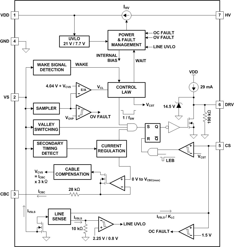
7.3 Feature Description
7.3.1 Primary-Side Regulation (PSR)
Figure 13 illustrates a simplified isolated-flyback convertor with the main voltage regulation blocks of the device shown. The power train operation is the same as any DCM flyback circuit but accurate output voltage and current sensing is the key to primary-side control. The output voltage is sensed as a reflected voltage during the transformer demagnetization time using a divider network at the VS input. The primary winding current is sensed at the CS input using a current-sense resistor, RCS.
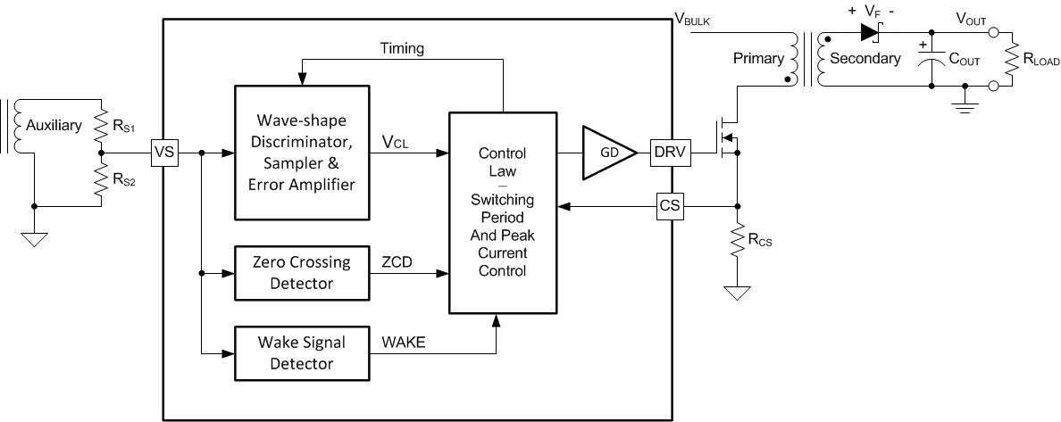 Figure 13. Simplified Flyback Convertor (with the main voltage regulation blocks)
In primary-side control, the output voltage is indirectly sensed on the auxiliary winding at the end of the transfer of stored transformer energy to the secondary. As shown in Figure 14 it is clear there is a down slope representing a decreasing total rectifier VF and resistance voltage drop as the secondary current decreases to zero. To achieve an accurate representation of the secondary output voltage on the auxiliary winding, the discriminator reliably blocks the leakage inductance reset and ringing, continuously samples the auxiliary voltage during the down slope after the ringing is diminished, and captures the error signal at the time the secondary winding reaches zero current. The internal reference on VS is 4.04 V. Temperature compensation on the VS reference voltage of -1 mV/°C offsets the change in the forward voltage of the output rectifier with temperature. The resistor divider is selected as outlined in the VS pin description.
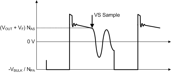 Figure 14. Auxiliary Winding Voltage
The UCC28730 VS-signal sampler includes signal discrimination methods to ensure an accurate sample of the output voltage from the auxiliary winding. There are, however, some details of the auxiliary winding signal which require attention to ensure reliable operation, specifically the reset time of the leakage inductance and the duration of any subsequent leakage inductance ring. Refer to Figure 15 below for a detailed illustration of waveform criteria to ensure a reliable sample on the VS pin.
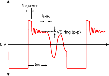 Figure 15. Auxiliary Waveform Details
The first detail to examine is the duration of the leakage inductance reset pedestal, tLK_RESET in Figure 15. Since this can mimic the waveform of the secondary current decay, followed by a sharp downslope, it is important to keep the leakage reset time to less than 750 ns for IPRI minimum, and to less than 2.25 µs for IPRI maximum.
The second detail is the amplitude of ringing on the VAUX waveform following tLK_RESET. The peak-to-peak voltage at the VS pin should be less than 125 mV for at least 200 ns before the end of the demagnetization time, tDM. If there is a concern with excessive ringing, it usually occurs during light-load or no-load conditions, when tDM is at the minimum. To avoid distorting the signal waveform at VS with oscilloscope probe capacitance, it is recommended to probe the auxiliary winding to view the VS waveform characteristics. The tolerable ripple on VS is scaled up to the auxiliary-winding voltage by RS1 and RS2, and is equal to 125 mV x (RS1 + RS2) / RS2.
7.3.2 Primary-Side Constant Voltage Regulation
During voltage regulation, the controller operates in frequency modulation and amplitude modulation modes according to the control law as illustrated in Figure 16 below. The control law voltage VCL reflects the internal operating level based on the voltage-error amplifier output signal. Neither of these signals is accessible to the user, however the approximate VCL may be inferred from the frequency and amplitude of the current sense signal at the CS input. As the line and load conditions vary, VCL adjusts the operating frequency and amplitude as required to maintain regulation of the output voltage. Because the UCC28730 incorporates internal loop compensation, no external stability compensation is required.
The internal operating frequency limits of the device are fSW(max) and fSW(min), typically 83.3 kHz and 32 Hz, respectively. The choice of transformer primary inductance and primary-peak current sets the maximum operating frequency of the converter, which must be equal to or lower than fSW(max). Conversely, the choice of maximum target operating frequency and primary-peak current determines the transformer primary-inductance value. The actual minimum switching frequency for any particular converter depends on several factors, including minimum loading level, leakage inductance losses, switched-node capacitance losses, other switching and conduction losses, and bias-supply requirements. In any case, the minimum steady-state frequency of the converter must always exceed fSW(min) or the output voltage may rise to the overvoltage protection level (OVP) and the controller responds as described in the Fault Protection Section.
The steady-state Control-Law voltage, VCL, ranges between 1.3 to 4.85 V, depending on load, but may occasionally move below 0.75 V or above 4.85 V on load transients. Dropping below 0.75 V shifts the switching frequency to a lower range at light loads, while exceeding 4.85 V enters the constant-current mode of operation. There are 3 lower operating frequency ranges for progressively lighter loads, each overlapping the previous range to some extent, to provide stable regulation at very low frequencies. Peak-primary current is always maintained at IPP(max)/3 in these lower frequency levels. Transitions between levels is automatically accomplished by the controller depending on the internal control-law voltage, VCL.
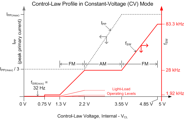 Figure 16. Frequency and Amplitude Modulation Modes (during voltage regulation)
7.3.3 Primary-Side Constant Current Regulation
Timing information at the VS pin and current information at the CS pin allow accurate regulation of the secondary average current. The control law dictates that as power is increased in CV regulation and approaching CC regulation the primary-peak current will be at IPP(max). Referring to Figure 17 below, the primary-peak current, turns ratio, secondary demagnetization time (tDM), and switching period (tSW) determine the secondary average output current. Ignoring leakage inductance effects, the average output current is given by Equation 6.
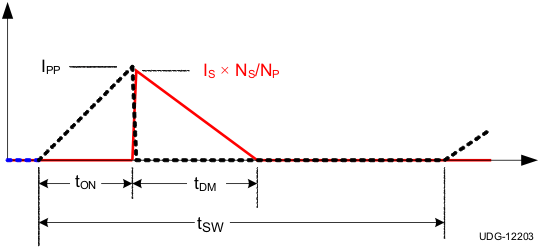 Figure 17. Transformer Currents Relationship

When the average output current reaches the CC regulation reference in the current control block, the controller operates in frequency modulation mode to control the output current, IOCC, at any output voltage down to or below the minimum operating voltage target, VOCC (as seen in Figure 18), as long as the auxiliary winding can keep VDD voltage above the UVLO turn-off threshold. When VO falls so low that VDD cannot be sustained above UVLO, the device shuts down.
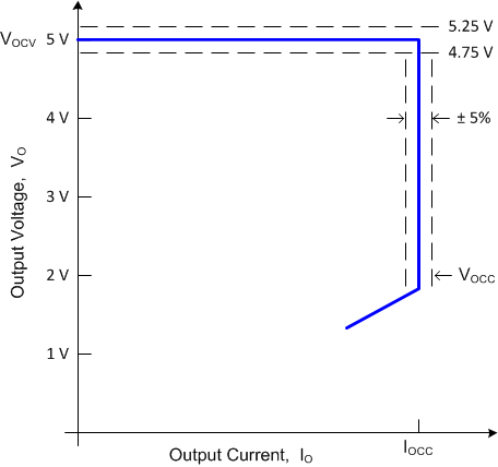 Figure 18. Typical Output V-I Target Characteristic
7.3.4 Wake-Up Detection and Function
A major feature available at the VS pin is the wake-up function which operates in conjunction with a companion secondary-side wake-up device, such as the UCC24650. This feature allows light-load and no-load switching frequencies to approach 32 Hz to minimize losses, yet wake the UCC28730 from its wait state (sleep mode) in the event of a significant load step between power cycles. Despite the low frequencies, excessive output capacitance is not required to maintain reasonable transient response. While in the wait state, the UCC28730 continually monitors the VS input for a wake-up signal, and when detected, responds immediately with several high-frequency power cycles and resumes operation as required by the control law to recover from the load-step transient and restore output voltage regulation.
Because the wake-up feature interrupts the wait state between very low frequency switching cycles, it allows the use of a much lower output capacitance value than would be required to hold up the voltage without the wake-up function. It also allows the controller to drop to extremely low switching frequencies at no-load conditions to minimize switching losses. This facilitates the achievement of less than 5 mW of input power to meet zero-power stand-by requirements. Use of the UCC28730 controller alone cannot ensure zero-power operation since other system-level limitations are also imposed, however, the UCC28730 and UCC24650 combination goes a long way to reaching this goal.
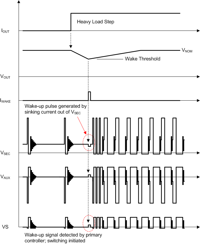 Figure 19. Simplified Wake-Up Operation and Waveforms
The signals illustrated in Figure 19 refer to circuit nodes located on the 简化电路原理图 diagram on the first page of this datasheet. The wake-up signal, which is provided by a secondary-side driver, must meet certain criteria to be considered valid and recognized by the UCC28730 at the VS input. To distinguish the signal from the residual resonant ringing that follows a switching power cycle, the resonant ringing amplitude must diminish and remain below the wake-up signal detection threshold, VWU, for a fixed qualification time, tWUDLY.
The UCC28730 has two such thresholds; one at VWU(low) and one at VWU(high). The lower VWU(low) threshold is used by converters which incorporate a relatively high-impedance driver for the wake-up signal, while the upper VWU(high) threshold may be used in converters with a low-impedance wake-up driver. Both thresholds work exactly the same way. The advantage of the upper threshold is that the UCC28730 is qualified to accept a strong wake-up signal without waiting additional time for the resonant ringing to diminish below the lower threshold.
Figure 20 illustrates the qualification delay period and wake-up response to a low-level wake-up signal. Figure 21 illustrates the qualification delay period and wake-up response to a high-level wake-up signal.
 Figure 20. Wake-Up Qualification Criteria and Wake-Up Response with Low Wake-Up Signal
 Figure 21. Wake-Up Qualification Criteria and Wake-Up Response with High Wake-Up Signal
7.3.5 Valley-Switching and Valley-Skipping
The UCC28730 utilizes valley-switching to reduce switching losses in the MOSFET, to reduce induced-EMI, and to minimize the turn-on current spike at the current-sense resistor. The controller operates in valley-switching in all load conditions unless the VDS ringing is diminished to the point where valleys are no longer detectable.
As shown in Figure 22, the UCC28730 operates in a valley-skipping mode (also known as valley-hopping) in most load conditions to maintain an accurate voltage or current regulation point and still switch on the lowest available VDS voltage.
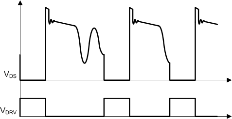 Figure 22. Valley-Skipping Mode
Valley-skipping modulates each switching cycle into discrete period durations. During FM operation, the switching cycles are periods when energy is delivered to the output in fixed packets, and the power delivered varies inversely with the switching period. During operating conditions when the switching period is relatively short, such as at high-load and low-line, the average power delivered per cycle varies significantly based on the number of valleys skipped between cycles. As a consequence, valley-skipping adds additional low-amplitude ripple voltage to the output with a frequency dependent upon the rate of change of the bulk voltage. For a load with an average power level between that of cycles with fewer valleys skipped and cycles with more valleys skipped, the voltage-control loop modulates the control law voltage and toggles between longer and shorter switching periods to match the required average output power.
7.3.6 Startup Operation
An internal high-voltage startup switch, connected to the bulk capacitor voltage (VBULK) through the HV pin, charges the VDD capacitor. This startup switch functions similarly to a current source providing typically 250 µA to charge the VDD capacitor. When VVDD reaches the 21-V UVLO turn-on threshold, the controller is enabled, the converter starts switching, and the startup switch turns off.
At initial turn-on, the output capacitor is often in a fully-discharged state. The first 4 switching-cycle current peaks are limited to IPP(min) to monitor for any initial input or output faults with limited power delivery. After these 4 cycles, if the sampled voltage at VS is less than 1.32 V, the controller operates in a special startup mode. In this mode, the primary-current-peak amplitude of each switching cycle is limited to approximately 0.67 x IPP(max) and DMAGCC increases from 0.432 to 0.650. These modifications to IPP(max) and DMAGCC during startup allow high-frequency charge-up of the output capacitor to avoid audible noise while the demagnetization voltage is low. Once the sampled VS voltage exceeds 1.36 V, DMAGCC is restored to 0.432 and the primary-current peak resumes as IPP(max). While the output capacitor charges, the converter operates in CC mode to maintain a constant output current until the output voltage enters regulation. Thereafter, the controller responds to conditions as dictated by the control law. The time to reach output regulation consists of the time the VDD capacitor charges to VVDD(on) plus the time the output capacitor charges.
7.3.7 Fault Protection
The UCC28730 provides comprehensive fault protection. The protection functions include:
- Output Overvoltage
- Input Undervoltage
- Internal Overtemperature
- Primary Overcurrent fault
- CS-pin Fault
- VS-pin Fault
A UVLO reset and restart sequence applies to all fault-protection events.
The output-overvoltage function is determined by the voltage feedback on the VS pin. If the voltage sample of VS exceeds 4.6 V for three consecutive switching cycles, the device stops switching and the internal current consumption becomes IFAULT which discharges the VDD capacitor to the UVLO-turn-off threshold. After that, the device returns to the start state and a start-up sequence ensues.
Current into the VS pin during the MOSFET on time determines the line-input run and stop voltages. While the VS pin clamps close to GND during the MOSFET on time, the current through RS1 is monitored to determine a sample of VBULK. A wide separation of the run and stop thresholds allows clean start-up and shut-down of the power supply with line voltage. The run-current threshold is 225 µA and the Stop-current threshold is 80 µA. The input AC voltage to run at start-up always corresponds to the peak voltage of the rectified line, because there is no loading on CBULK before start-up. The AC input voltage to stop varies with load since the minimum VBULK depends on the loading and the value of CBULK. At maximum load, the stop voltage is close to the run voltage, but at no-load condition the stop voltage can be approximately 1/3 of the run voltage.
The UCC28730 always operates with cycle-by-cycle primary-peak current control. The normal operating range of the CS pin is 0.74 to 0.249 V. An additional protection occurs if the CS pin reaches 1.5 V after the leading-edge blanking interval for three consecutive cycles, which results in a UVLO reset and restart sequence.
Normally at initial start-up, the peak level of the primary current of the first four power cycles is limited to the minimum VCST(min). If the CS input is shorted or held low such that the VCST(min) level is not reached within 4 µs on the first cycle, the CS input is presumed to be shorted to GND and the fault protection function results in a UVLO reset and restart sequence. Similarly, if the CS input is open, the internal voltage is pulled up to 1.5 V for three consecutive switching cycles and the fault protection function results in a UVLO reset and restart sequence.
The internal overtemperature-protection threshold is 165°C. If the junction temperature reaches this threshold, the device initiates a UVLO-reset cycle. If the temperature is still high at the end of the UVLO cycle, the protection cycle repeats.
Protection is included in the event of component failures on the VS pin. If complete loss of feedback information on the VS pin occurs, the controller stops switching and restarts.
7.4 Device Functional Modes
According to the input voltage, the VDD voltage, and the output load conditions, the device can operate in different modes:
- At start-up, when VDD is less than the VVDD(on) turn-on threshold, the HV internal current source is on and charging the VDD capacitor at a (IHV – ISTART) rate.
- When VDD exceeds VVDD(on), the HV source is turned Off and the device starts switching to deliver power to the converter output. Depending on the load conditions, the converter operates in CC mode or CV mode.
- CC mode means that the converter keeps the output current constant. When the output voltage is below the regulation level, the converter operates in CC mode to restore the output to the regulation voltage.
- CV mode means that the converter keeps the output voltage constant. When the load current is less than the current limit level, the converter operates in CV mode to keep the output voltage at the regulation level over the full load and input line ranges.
- When operating in CV or CC mode where IPP is greater than 0.55 X IPP(max), the UCC28730 operates continuously in the run state. In this state, the VDD bias current is always at IRUN plus the average gate-drive current.
- When operating in CV mode where IPP is less than 0.55 X IPP(max), the UCC28730 operates in the Wait state between switching cycles and in the run state during a switching cycle. In the Wait state, the VDD bias current is reduced to IWAIT after each switching cycle to improve efficiency at light loads.
- The device operation can be stopped by the events listed below:
- If VDD drops below the VVDD(off) threshold, the device stops switching, its bias current consumption is lowered to ISTART and the internal HV current source is turned on until VDD rises above the VVDD(on) threshold. The device then resumes switching.
- If a fault condition is detected, the device stops switching and its bias current consumption is lowered to IFAULT. This current level slowly the discharges VDD to VVDD(off) where the bias current changes from IFAULT to ISTART and the internal HV current source is turned on until VDD rises above the VVDD(on) threshold.
- If a fault condition persists, the operation sequence described above in (2) repeats until the fault condition or the input voltage is removed.