ZHCSEQ1A February 2016 – February 2016 UCC28704
PRODUCTION DATA.
- 1 特性
- 2 应用
- 3 说明
- 4 修订历史记录
- 5 Pin Configuration and Functions
- 6 Specifications
-
7 Detailed Description
- 7.1 Overview
- 7.2 Functional Block Diagram
- 7.3
Feature Description
- 7.3.1 Detailed Pin Description
- 7.3.2 Primary-Side Regulation (PSR)
- 7.3.3 Primary-Side Constant Voltage (CV) Regulation
- 7.3.4 Primary-Side Constant Current (CC) Regulation
- 7.3.5 Valley-Switching and Valley-Skipping
- 7.3.6 Start-Up Operation
- 7.3.7 Fault Protection
- 7.3.8 Constant Current Under-Voltage Protection
- 7.3.9 Load Transient Response
- 7.4 Device Functional Modes
-
8 Applications and Implementation
- 8.1 Application Information
- 8.2
Typical Application
- 8.2.1 Design Requirements
- 8.2.2
Detailed Design Procedure
- 8.2.2.1 VDD Capacitance, CDD
- 8.2.2.2 VDD Start-Up Resistance, RSTR
- 8.2.2.3 Input Bulk Capacitance and Minimum Bulk Voltage
- 8.2.2.4 Transformer Turns Ratio, Inductance, Primary-Peak Current
- 8.2.2.5 Transformer Parameter Verification
- 8.2.2.6 VS Resistor Divider, Line Compensation, and NTC
- 8.2.2.7 Standby Power Estimate
- 8.2.2.8 Output Capacitance
- 8.2.2.9 Design Considerations in Using with Synchronous Rectifiers
- 8.2.3 Application Curves
- 8.3 Do's and Don'ts
- 9 Power Supply Recommendations
- 10Layout
- 11器件和文档支持
- 12机械、封装和可订购信息
10 Layout
10.1 Layout Guidelines
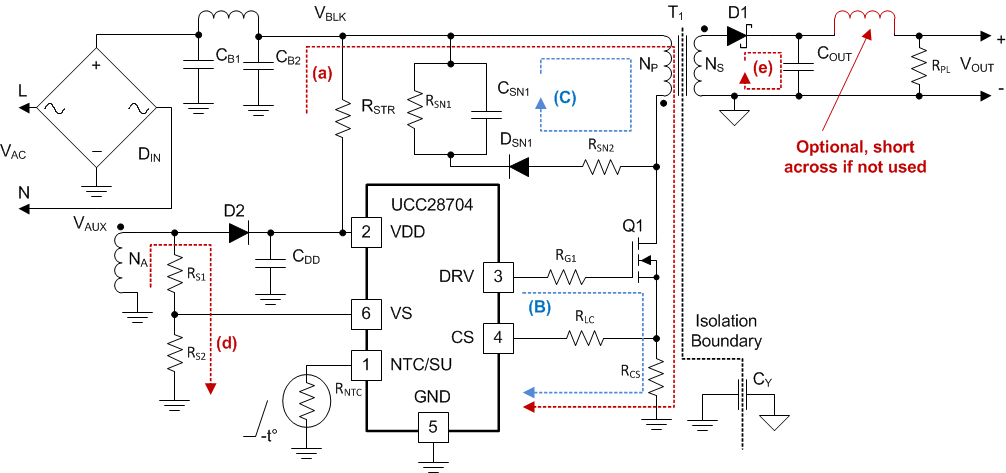
In order to increase the reliability and feasibility of the project it is recommended to adhere to the following guidelines for PCB layout. In Figure 32, a typical 5-V/2-A USB adapter design schematic is shown in Figure 32.
- Minimize stray capacitance on the VS node. Place the voltage sense resistors (RS1 and RS2 in Figure 24) close to the VS pin.
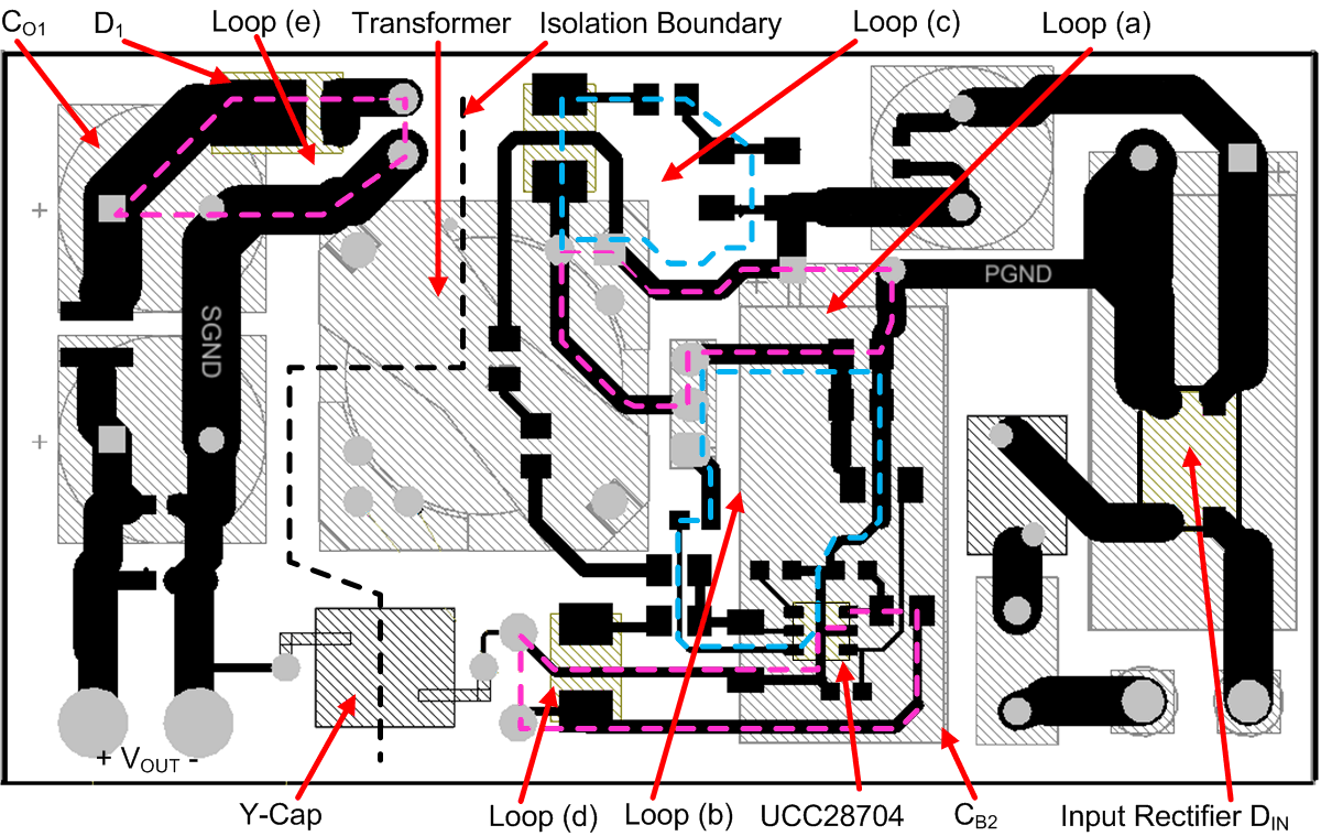
- Arrange the components to minimize the loop areas of the switching currents as much as possible. These areas include such loops as the transformer primary winding current loop (a), the MOSFET gate-drive loop (b), the primary snubber loop (c), the auxiliary winding loop (d) and the secondary output current loop (e). In practice, trade-offs may have to be made. Loops with higher current should be minimized with higher priority. As a rule of thumb, the priority goes from high to low as (a) – (e) – (c) – (d) – (b).
- The RLC resistor location is critical. To avoid any dv/dt induced noise (for example MOSFET drain dv/dt) coupled onto this resistor, it is better to place RLC closer to the controller and avoid nearby the MOSFET.
- To improve thermal performance increase the copper area connected to GND pins.
 Figure 32. 10-W, 5-V/2-A USB Adapter Schematics
10.2 Layout Example
Figure 33 demonstrates a 10-W, 5-V/2-A, layout with trade-offs to minimize the loops while effectively placing components and tracks for low noise operation on a single-layer printed circuit board. In addition to the consideration of minimal loops, one another layout guideline is always to use the device GND as reference point. This applies to both power and signal to return to the device GND pin (pin 5).
 Figure 33. Layout Example