SLUSB41A July 2012 – December 2014 UCC28700 , UCC28701 , UCC28702 , UCC28703
PRODUCTION DATA.
- 1 Features
- 2 Applications
- 3 Description
- 4 Revision History
- 5 Device Comparison Table
- 6 Pin Configuration and Functions
- 7 Specifications
- 8 Detailed Description
-
9 Applications and Implementation
- 9.1 Application Information
- 9.2
Typical Application
- 9.2.1 Design Requirements
- 9.2.2
Detailed Design Procedure
- 9.2.2.1 Transformer Parameter Verification
- 9.2.2.2 Output Capacitance
- 9.2.2.3 VDD Capacitance, CDD
- 9.2.2.4 VDD Start-Up Resistance, RSTR
- 9.2.2.5 VS Resistor Divider, Line Compensation, and Cable Compensation
- 9.2.2.6 Input Bulk Capacitance and Minimum Bulk Voltage
- 9.2.2.7 Transformer Turns Ratio, Inductance, Primary-Peak Current
- 9.2.2.8 Standby Power Estimate
- 9.2.3 Application Curves
- 10Power Supply Recommendations
- 11Layout
-
12Device and Documentation Support
- 12.1
Device Support
- 12.1.1
Device Nomenclature
- 12.1.1.1 Capacitance Terms in Farads
- 12.1.1.2 Duty Cycle Terms
- 12.1.1.3 Frequency Terms in Hertz
- 12.1.1.4 Current Terms in Amperes
- 12.1.1.5 Current and Voltage Scaling Terms
- 12.1.1.6 Transformer Terms
- 12.1.1.7 Power Terms in Watts
- 12.1.1.8 Resistance Terms in Ω
- 12.1.1.9 Timing Terms in Seconds
- 12.1.1.10 Voltage Terms in Volts
- 12.1.1.11 AC Voltage Terms in VRMS
- 12.1.1.12 Efficiency Terms
- 12.1.1
Device Nomenclature
- 12.2 Documentation Support
- 12.3 Trademarks
- 12.4 Electrostatic Discharge Caution
- 12.5 Glossary
- 12.1
Device Support
- 13Mechanical, Packaging, and Orderable Information
1 Features
- < 30-mW No-Load Power for 5-Star Rating
- Primary-Side Regulation (PSR) Eliminates Opto-Coupler
- ±5% Voltage and Current Regulation
- 130-kHz Maximum Switching Frequency Enables High-Power Density Charger Designs
- Quasi-Resonant Valley-Switching Operation for Highest Overall Efficiency
- Patent-Pending Frequency-Jitter Scheme to Ease EMI Compliance
- Wide VDD Range Allows Small Bias Capacitor
- Clamped Gate-Drive Output for MOSFET
- Protection Functions: Overvoltage, Low-Line, and Overcurrent
- Programmable Cable Compensation (UCC28700 Only)
- NTC Resistor Interface (UCC28701, UCC28702 and UCC28703 Only) With Fixed Cable Compensation Options
- SOT-23 Package
2 Applications
- USB-Compliant Adapters and Chargers for Consumer Electronics (Cell Phones, Tablets and Cameras)
- AC and DC Power Supplies
3 Description
The UCC28700 family of flyback power supply controllers provides Constant-Voltage (CV) and Constant-Current (CC) output regulation without the use of an optical coupler. The devices process information from the primary power switch and an auxiliary flyback winding for precise control of output voltage and current. Low start-up current, dynamically controlled operating states and a tailored modulation profile support very low standby power without sacrificing start-up time or output transient response.
Control algorithms in the UCC28700 family allow operating efficiencies to meet or exceed applicable standards. The output drive interfaces to a MOSFET power switch. Discontinuous Conduction Mode (DCM) with valley switching reduces switching losses. Modulation of switching frequency and primary current peak amplitude (FM and AM) keeps the conversion efficiency high across the entire load and line ranges.
The controllers have a maximum switching frequency of 130 kHz and always maintain control of the peak-primary current in the transformer. Protection features help keep primary and secondary component stresses in check. The UCC28700 allows the level of cable compensation to be programmed. The UCC28701, UCC28702, and UCC28703 devices allow remote temperature sensing using a Negative Temperature Coefficient (NTC) resistor while providing fixed cable-compensation levels.
Device Information(1)
| PART NUMBER | PACKAGE | BODY SIZE (NOM) |
|---|---|---|
| UCC28700 | SOT-23 (6) | 2.90 mm × 1.60 mm |
| UCC28701 | ||
| UCC28702 | ||
| UCC28703 |
- For all available packages, see the orderable addendum at the end of the datasheet.
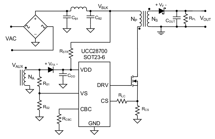
Typical Application Schematic