SLUSB41A July 2012 – December 2014 UCC28700 , UCC28701 , UCC28702 , UCC28703
PRODUCTION DATA.
- 1 Features
- 2 Applications
- 3 Description
- 4 Revision History
- 5 Device Comparison Table
- 6 Pin Configuration and Functions
- 7 Specifications
- 8 Detailed Description
-
9 Applications and Implementation
- 9.1 Application Information
- 9.2
Typical Application
- 9.2.1 Design Requirements
- 9.2.2
Detailed Design Procedure
- 9.2.2.1 Transformer Parameter Verification
- 9.2.2.2 Output Capacitance
- 9.2.2.3 VDD Capacitance, CDD
- 9.2.2.4 VDD Start-Up Resistance, RSTR
- 9.2.2.5 VS Resistor Divider, Line Compensation, and Cable Compensation
- 9.2.2.6 Input Bulk Capacitance and Minimum Bulk Voltage
- 9.2.2.7 Transformer Turns Ratio, Inductance, Primary-Peak Current
- 9.2.2.8 Standby Power Estimate
- 9.2.3 Application Curves
- 10Power Supply Recommendations
- 11Layout
-
12Device and Documentation Support
- 12.1
Device Support
- 12.1.1
Device Nomenclature
- 12.1.1.1 Capacitance Terms in Farads
- 12.1.1.2 Duty Cycle Terms
- 12.1.1.3 Frequency Terms in Hertz
- 12.1.1.4 Current Terms in Amperes
- 12.1.1.5 Current and Voltage Scaling Terms
- 12.1.1.6 Transformer Terms
- 12.1.1.7 Power Terms in Watts
- 12.1.1.8 Resistance Terms in Ω
- 12.1.1.9 Timing Terms in Seconds
- 12.1.1.10 Voltage Terms in Volts
- 12.1.1.11 AC Voltage Terms in VRMS
- 12.1.1.12 Efficiency Terms
- 12.1.1
Device Nomenclature
- 12.2 Documentation Support
- 12.3 Trademarks
- 12.4 Electrostatic Discharge Caution
- 12.5 Glossary
- 12.1
Device Support
- 13Mechanical, Packaging, and Orderable Information
8 Detailed Description
8.1 Overview
The UCC28700 is a flyback power supply controller which provides accurate voltage and constant current regulation with primary-side feedback, eliminating the need for opto-coupler feedback circuits. The controller operates in discontinuous conduction mode with valley-switching to minimize switching losses. The modulation scheme is a combination of frequency and primary peak current modulation to provide high conversion efficiency across the load range. The control law provides a wide-dynamic operating range of output power to achieve the <30-mW stand-by power requirement.
Another feature beneficial to achieve low stand-by power without excessive start-up time is a wide operating VDD range to allow a high-value VDD start-up resistance and low-value VDD capacitance. During low-power operating ranges the device has power management features to reduce the device operating current at operating frequencies below 44 kHz. The UCC28700 controller includes features in the modulator to reduce the EMI peak energy of the fundamental switching frequency and harmonics. Accurate voltage and constant current regulation, fast dynamic response, and fault protection are achieved with primary-side control. A complete charger solution can be realized with a straightforward design process, low cost and low component count.
8.2 Functional Block Diagram
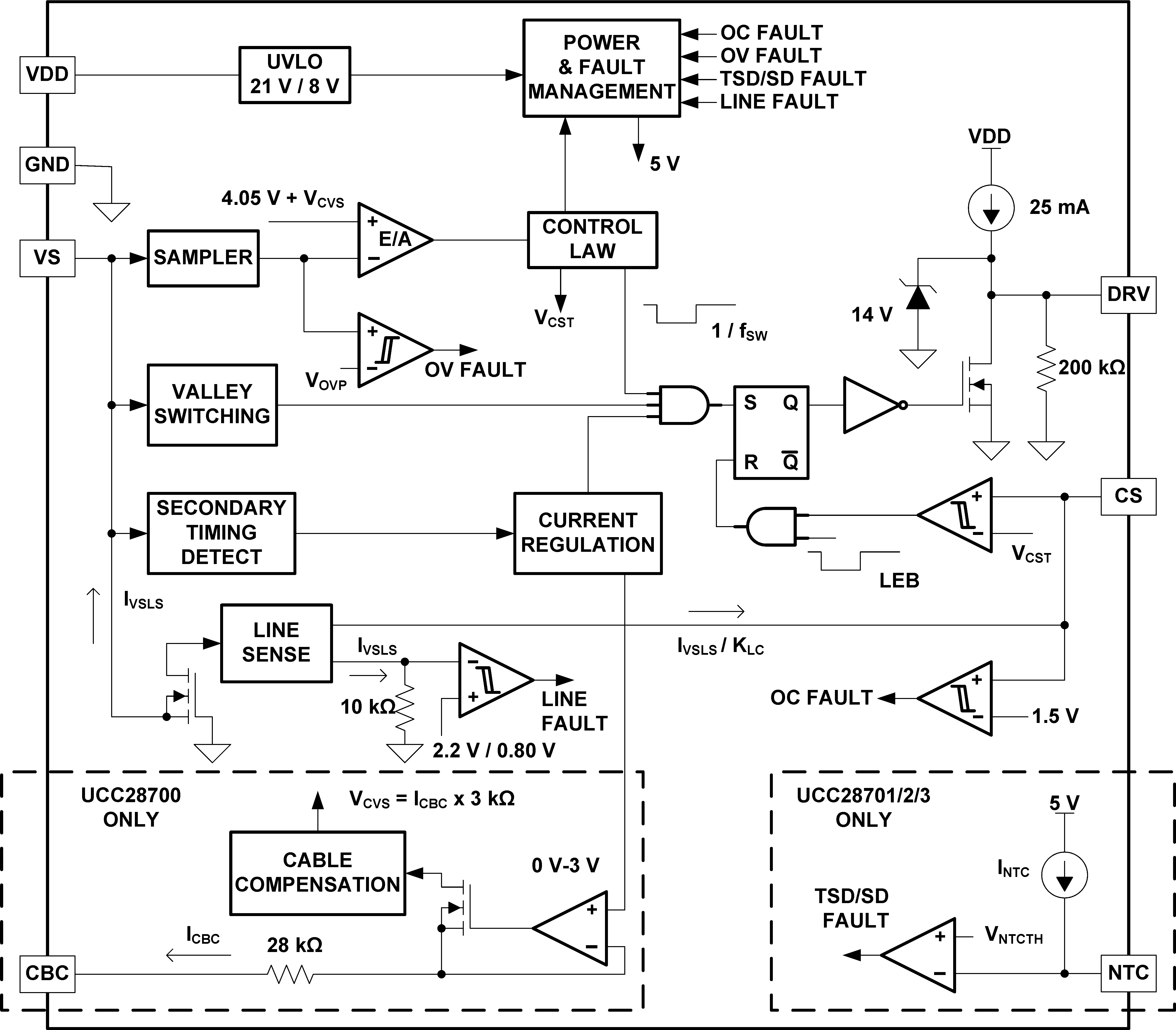
8.3 Feature Description
8.3.1 Detailed Pin Description
8.3.1.1 VDD (Device Bias Voltage Supply)
The VDD pin is connected to a bypass capacitor to ground and a start-up resistance to the input bulk capacitor (+) terminal. The VDD turn-on UVLO threshold is 21 V and turn-off UVLO threshold is 8.1 V, with an available operating range up to 35 V. The USB charging specification requires the output current to operate in constant-current mode from 5 V to a minimum of 2 V; this is easily achieved with a nominal VDD of approximately 25 V. The additional VDD headroom up to 35 V allows for VDD to rise due to the leakage energy delivered to the VDD capacitor in high-load conditions. Also, the wide VDD range provides the advantage of selecting a relatively small VDD capacitor and high-value start-up resistance to minimize no-load stand-by power loss in the start-up resistor.
8.3.1.2 GND (Ground)
This is a single ground reference external to the device for the gate drive current and analog signal reference. Place the VDD bypass capacitor close to GND and VDD with short traces to minimize noise on the VS and CS signal pins.
8.3.1.3 VS (Voltage-Sense)
The VS pin is connected to a resistor divider from the auxiliary winding to ground. The output-voltage feedback information is sampled at the end of the transformer secondary current demagnetization time to provide an accurate representation of the output voltage. Timing information to achieve valley-switching and to control the duty cycle of the secondary transformer current is determined by the waveform on the VS pin. Avoid placing a filter capacitor on this input which would interfere with accurate sensing of this waveform.
The VS pin also senses the bulk capacitor voltage to provide for AC-input run and stop thresholds, and to compensate the current-sense threshold across the AC-input range. This information is sensed during the MOSFET on-time. For the AC-input run/stop function, the run threshold on VS is 220 µA and the stop threshold is 80 µA. The values for the auxilliary voltage divider upper-resistor RS1 and lower-resistor RS2 can be determined by the equations below.
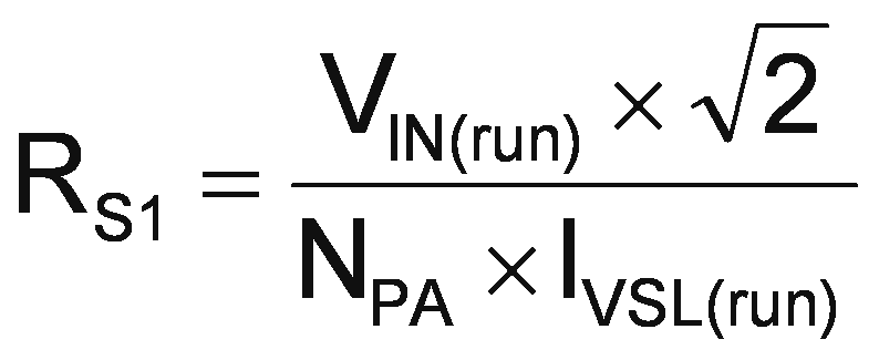
where
- NPA is the transformer primary-to-auxiliary turns ratio,
- VIN(run) is the AC RMS voltage to enable turn-on of the controller (run),
- IVSL(run) is the run-threshold for the current pulled out of the VS pin during the MOSFET on-time. (see the Electrical Characteristics table)
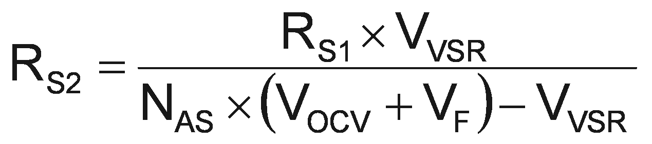
where
- VOCV is the converter regulated output voltage,
- VF is the output rectifier forward drop at near-zero current,
- NAS is the transformer auxiliary to secondary turns ratio,
- RS1 is the VS divider high-side resistance,
- VVSR is the CV regulating level at the VS input (see the Electrical Characteristics table).
8.3.1.4 DRV (Gate Drive)
The DRV pin is connected to the MOSFET gate pin, usually through a series resistor. The gate driver provides a gate-drive signal limited to 14 V. The turn-on characteristic of the driver is a 25-mA current source which limits the turn-on dv/dt of the MOSFET drain and reduces the leading-edge current spike, but still provides gate-drive current to overcome the Miller plateau. The gate-drive turn-off current is determined by the low-side driver RDS(on) and any external gate-drive resistance. The user can reduce the turn-off MOSFET drain dv/dt by adding external gate resistance.
8.3.1.5 CS (Current Sense)
The current-sense pin is connected through a series resistor (RLC) to the current-sense resistor (RCS). The current-sense threshold is 0.75 V for IPP(max) and 0.25 V for IPP(min). The series resistor RLC provides the function of feed-forward line compensation to eliminate change in IPP due to change in di/dt and the propagation delay of the internal comparator and MOSFET turn-off time. There is an internal leading-edge blanking time of 235 ns to eliminate sensitivity to the MOSFET turn-on current spike. It should not be necessary to place a bypass capacitor on the CS pin. The value of RCS is determined by the target output current in constant-current (CC) regulation. The values of RCS and RLC can be determined by the equations below. The term ηXFMR is intended to account for the energy stored in the transformer but not delivered to the secondary. This includes transformer resistance and core loss, bias power, and primary-to-secondary leakage ratio.
Example: With a transformer core and winding loss of 5%, primary-to-secondary leakage inductance of 3.5%, and bias power to output power ratio of 1.5%. The ηXFMR value is approximately: 1 - 0.05 - 0.035 - 0.015 = 0.9.
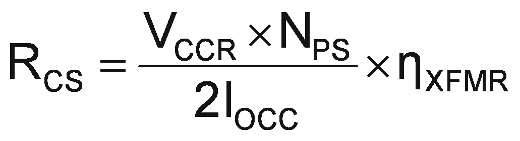
where
- VCCR is a current regulation constant (see the Electrical Characteristics table),
- NPS is the transformer primary-to-secondary turns ratio (a ratio of 13 to 15 is recommended for 5-V output),
- IOCC is the target output current in constant-current regulation,
- ηXFMR is the transformer efficiency.
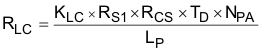
where
- RS1 is the VS pin high-side resistor value,
- RCS is the current-sense resistor value,
- TD is the current-sense delay including MOSFET turn-off delay, add ~50 ns to MOSFET delay,
- NPA is the transformer primary-to-auxiliary turns ratio,
- LP is the transformer primary inductance,
- KLC is a current-scaling constant (see the Electrical Characteristics table).
8.3.1.6 CBC (Cable Compensation), Pin 1 UCC28700
The cable compensation pin is connected to a resistor to ground to program the amount of output voltage compensation to offset cable resistance. The cable compensation block provides a 0-V to 3-V voltage level on the CBC pin corresponding to 0 to IOCC output current. The resistance selected on the CBC pin programs a current mirror that is summed into the VS feedback divider therefore increasing the output voltage as IOUT increases. There is an internal series resistance of 28 kΩ to the CBC pin which sets a maximum cable compensation of a 5-V output to 400 mV when CBC is shorted to ground. The CBC resistance value can be determined by the equation below.
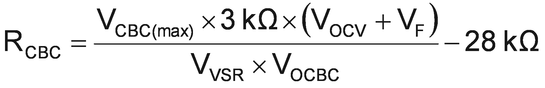
where
- VO is the output voltage,
- VF is the diode forward voltage,
- VOCBC is the target cable compensation voltage at the output terminals,
- VCBC(max) is the maximum voltage at the cable compensation pin at the maximum converter output current (see the Electrical Characteristics table),
- VVSR is the CV regulating level at the VS input (see the Electrical Characteristics table).
8.3.1.7 NTC (NTC Thermistor Shut-down), Pin 1 UCC28701/2/3
These versions of the UCC28700 family utilize pin 1 for an external NTC thermistor to allow user-programmable external thermal shut-down. The shut-down threshold is 0.95 V with an internal 105-µA current source which results in a 9.05-kΩ thermistor shut-down threshold. These controllers have either zero or fixed internal cable compensation.
8.3.2 Fault Protection
There is comprehensive fault protection incorporated into the UCC28700. Protection functions include:
- Output overvoltage
- Input undervoltage
- Internal overtemperature
- Primary overcurrent fault
- CS pin fault
- VS pin fault
A UVLO reset and restart sequence applies for all fault protection events.
The output over-voltage function is determined by the voltage feedback on the VS pin. If the voltage sample on VS exceeds 115% of the nominal VOUT, the device stops switching and keeps the internal circuitry enabled to discharge the VDD capacitor to the UVLO turn-off threshold. After that, the device returns to the start state and a start-up sequence ensues.
The UCC28700 always operates with cycle-by-cycle primary peak current control. The normal operating range of the CS pin is 0.75 V to 0.25 V. There is additional protection if the CS pin reaches 1.5 V. This results in a UVLO reset and restart sequence. There is no leading-edge blanking on the 1.5-V threshold on CS.
The line input run and stop thresholds are determined by current information at the VS pin during the MOSFET on-time. While the VS pin is clamped close to GND during the MOSFET on-time, the current through RS1 is monitored to determine a sample of the bulk capacitor voltage. A wide separation of run and stop thresholds allows clean start-up and shut-down of the power supply with the line voltage. The run current threshold is 220 µA and the stop current threshold is 80 µA.
The internal overtemperature protection threshold is 165°C. If the junction temperature reaches this threshold the device initiates a UVLO reset cycle. If the temperature is still high at the end of the UVLO cycle, the protection cycle repeats.
Protection is included in the event of component failures on the VS pin. If complete loss of feedback information on the VS pin occurs, the controller stops switching and restarts.
8.4 Device Functional Modes
8.4.1 Primary-Side Voltage Regulation
Figure 12 shows a simplified flyback convertor with the main voltage regulation blocks of the device shown. The power train operation is the same as any DCM flyback circuit but accurate output voltage and current sensing is the key to primary-side control.
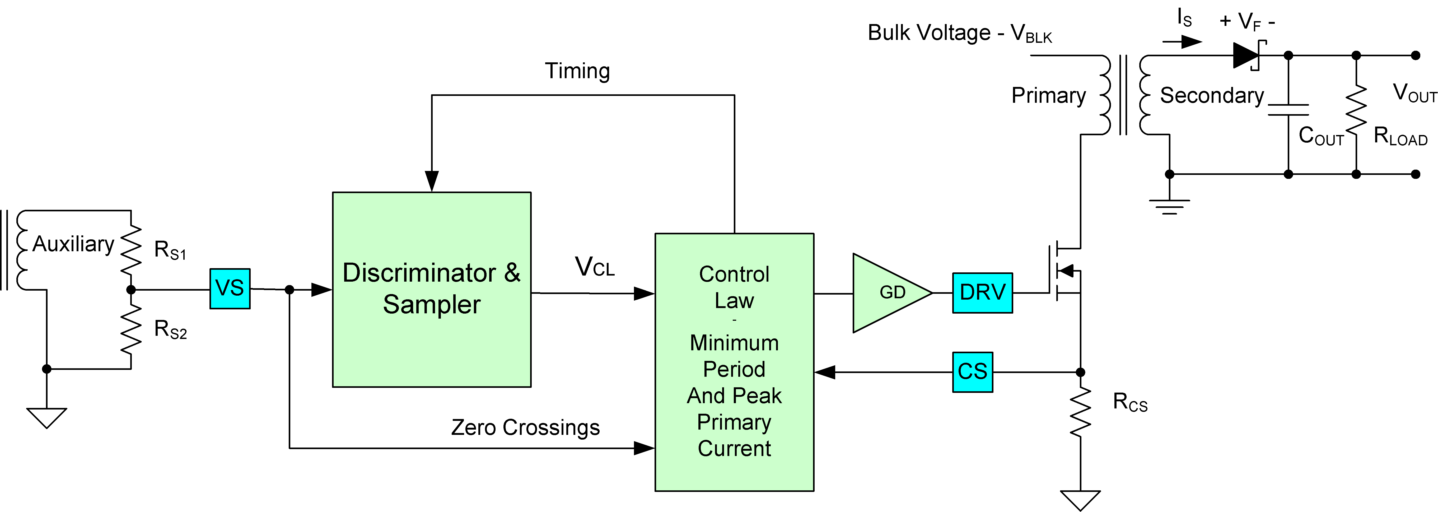 Figure 12. Simplified Flyback Convertor
 (with the main voltage regulation blocks)
In primary-side control, the output voltage is sensed on the auxiliary winding during the transfer of transformer energy to the secondary. As shown in Figure 13 it is clear there is a down slope representing a decreasing total rectifier VF and resistance voltage drop (ISRS) as the secondary current decreases to zero. To achieve an accurate representation of the secondary output voltage on the auxiliary winding, the discriminator reliably blocks the leakage inductance reset and ringing, continuously samples the auxiliary voltage during the down slope after the ringing is diminished, and captures the error signal at the time the secondary winding reaches zero current. The internal reference on VS is 4.05 V; the resistor divider is selected as outlined in the VS pin description.
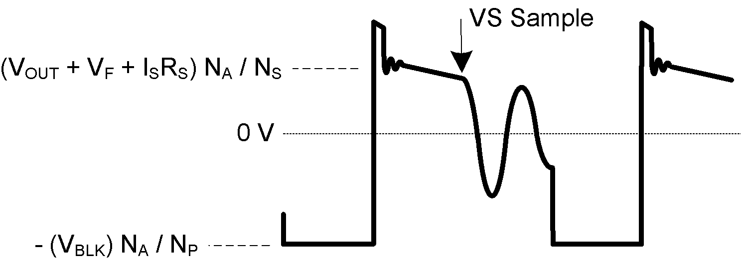 Figure 13. Auxiliary Winding Voltage
The UCC28700 VS signal sampler includes signal discrimination methods to ensure an accurate sample of the output voltage from the auxiliary winding. There are however some details of the auxiliary winding signal to ensure reliable operation, specifically the reset time of the leakage inductance and the duration of any subsequent leakage inductance ring. Refer to Figure 14 for a detailed illustration of waveform criteria to ensure a reliable sample on the VS pin. The first detail to examine is the duration of the leakage inductance reset pedestal, TLK_RESET in Figure 14. Because this can mimic the waveform of the secondary current decay, followed by a sharp downslope, it is important to keep the leakage reset time less than 500 ns for IPRI minimum, and less than 1.5 µs for IPRI maximum. The second detail is the amplitude of ringing on the VAUX waveform following TLK_RESET. The peak-to-peak voltage at the VS pin should be less than approximately 100 mVp-p at least 200 ns before the end of the demagnetization time, tDM. If there is a concern with excessive ringing, it usually occurs during light or no-load conditions, when tDM is at the minimum. The tolerable ripple on VS is scaled up to the auxiliary winding voltage by RS1 and RS2, and is equal to 100 mV x (RS1 + RS2) / RS2.
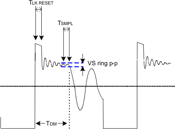 Figure 14. Auxiliary Waveform Details
During voltage regulation, the controller operates in frequency modulation mode and amplitude modulation mode as illustrated in Figure 15 below. The internal operating frequency limits of the device are 130 kHz maximum and 1 kHz minimum. The transformer primary inductance and primary peak current chosen sets the maximum operating frequency of the converter. The output preload resistor and efficiency at low power determines the converter minimum operating frequency. There is no stability compensation required for the UCC28700 controller.
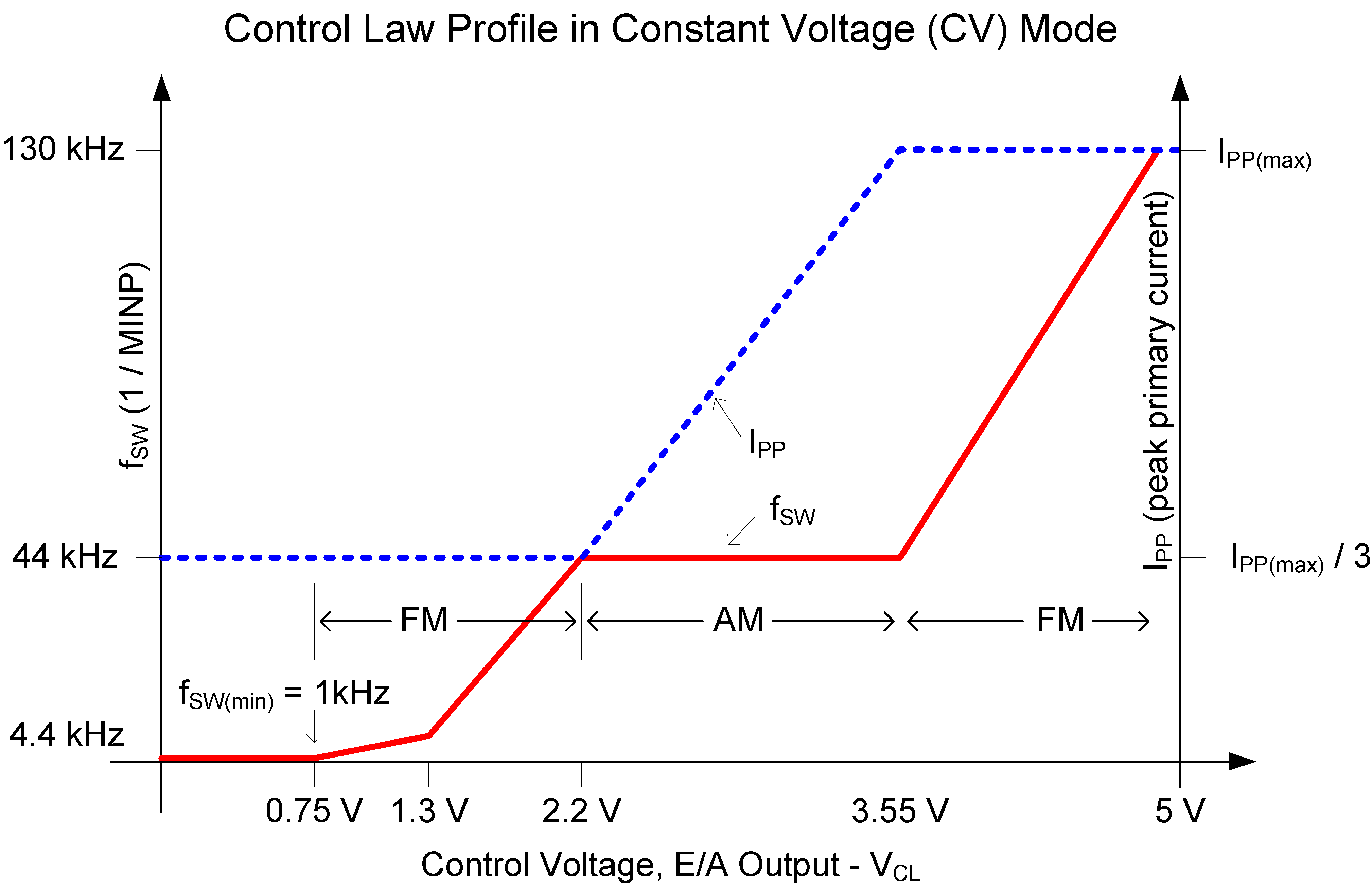 Figure 15. Frequency and Amplitude Modulation Modes
 (during voltage regulation)
8.4.2 Primary-Side Current Regulation
Timing information at the VS pin and current information at the CS pin allow accurate regulation of the secondary average current. The control law dictates that as power is increased in CV regulation and approaching CC regulation the primary-peak current is at IPP(max). Referring to Figure 16 below, the primary-peak current, turns ratio, secondary demagnetization time (tDM), and switching period (TSW) determine the secondary average output current. Ignoring leakage inductance effects, the average output current is given by Equation 6. When the average output current reaches the regulation reference in the current control block, the controller operates in frequency modulation mode to control the output current at any output voltage at or below the voltage regulation target as long as the auxiliary winding can keep VDD above the UVLO turn-off threshold.
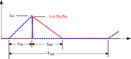 Figure 16. Transformer Currents
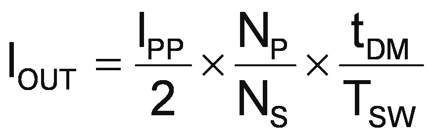
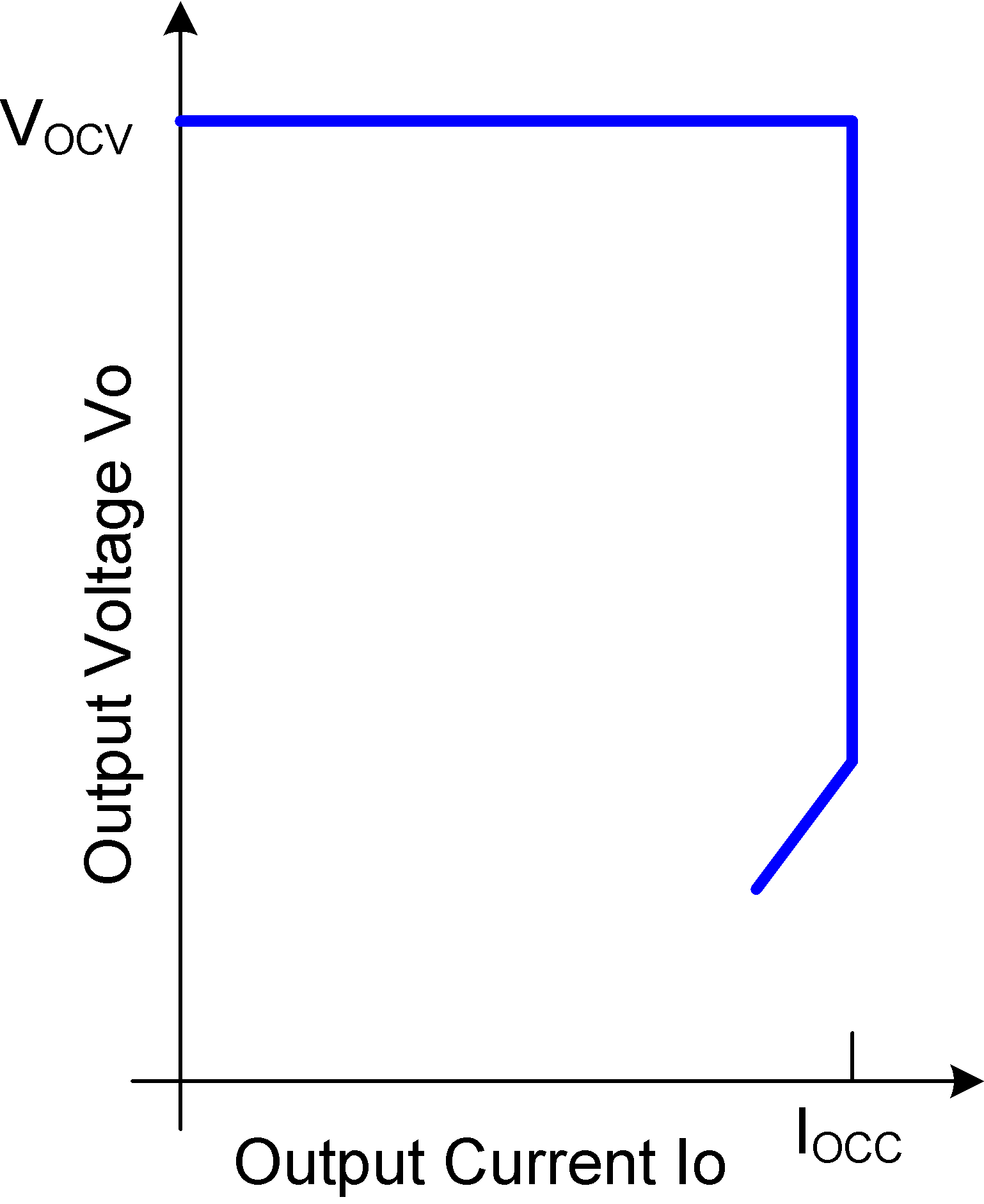 Figure 17. Typical Target Output V-I Characteristic
8.4.3 Valley-Switching
The UCC28700 utilizes valley-switching to reduce switching losses in the MOSFET, to reduce induced-EMI, and to minimize the turn-on current spike at the sense resistor. The controller operates in valley-switching in all load conditions unless the VDS ringing has diminished.
Referring to Figure 18 below, the UCC28700 operates in a valley-skipping mode in most load conditions to maintain an accurate voltage or current regulation point and still switch on the lowest available VDS voltage.
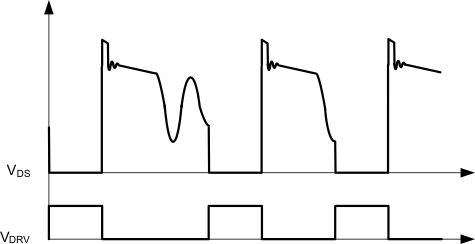 Figure 18. Valley-Skipping Mode
8.4.4 Start-Up Operation
Upon application of input voltage to the converter, the start-up resistor connected to VDD from the bulk capacitor voltage (VBLK) charges the VDD capacitor. During charging of the VDD capacitor the device bias supply current is less than 1.5 µA. When VDD reaches the 21-V UVLO turn-on threshold, the controller is enabled and the converter starts switching. The initial three cycles are limited to IPP(min). This allows sensing any initial input or output faults with minimal power delivery. After the initial three cycles at minimum IPP(min), the controller responds to the condition dictated by the control law. The converter remains in discontinuous mode during charging of the output capacitor(s), maintaining a constant output current until the output voltage is in regulation.