SLUS646K November 2005 – August 2015 UCC28600
PRODUCTION DATA.
- 1 Features
- 2 Applications
- 3 Description
- 4 Revision History
- 5 Pin Configuration and Functions
- 6 Specifications
- 7 Detailed Description
- 8 Application and Implementation
- 9 Power Supply Recommendations
- 10Layout
- 11Device and Documentation Support
- 12Mechanical, Packaging, and Orderable Information
10 Layout
10.1 Layout Guidelines
To increase the reliability and feasibility of the design it is recommended to adhere to the following guidelines for PCB layout.
- Minimize the high current loops to reduce parasitic capacitances and inductances. At the same time, do not inadvertently make traces with a high dv/dt too wide as this will create a very good E-field antenna.
- Separate the device signal ground from the high current power ground in order to isolate the noise away from the device substrate. The separate grounds should, ideally, be tied together at the input capacitor on the primary side.
- Return the sense resistor to the ground side of the input capacitor, instead of to the ground plane under the device.
- The bypass capacitor on VDD must be placed as close as possible to the VDD and GND pins of the device.
- The filter capacitor on CS must be placed as close as possible to the CS pin and GND pin of the device.
- The filter capacitor on FB must be placed as close as possible to the FB and GND pins of the device.
10.2 Layout Example
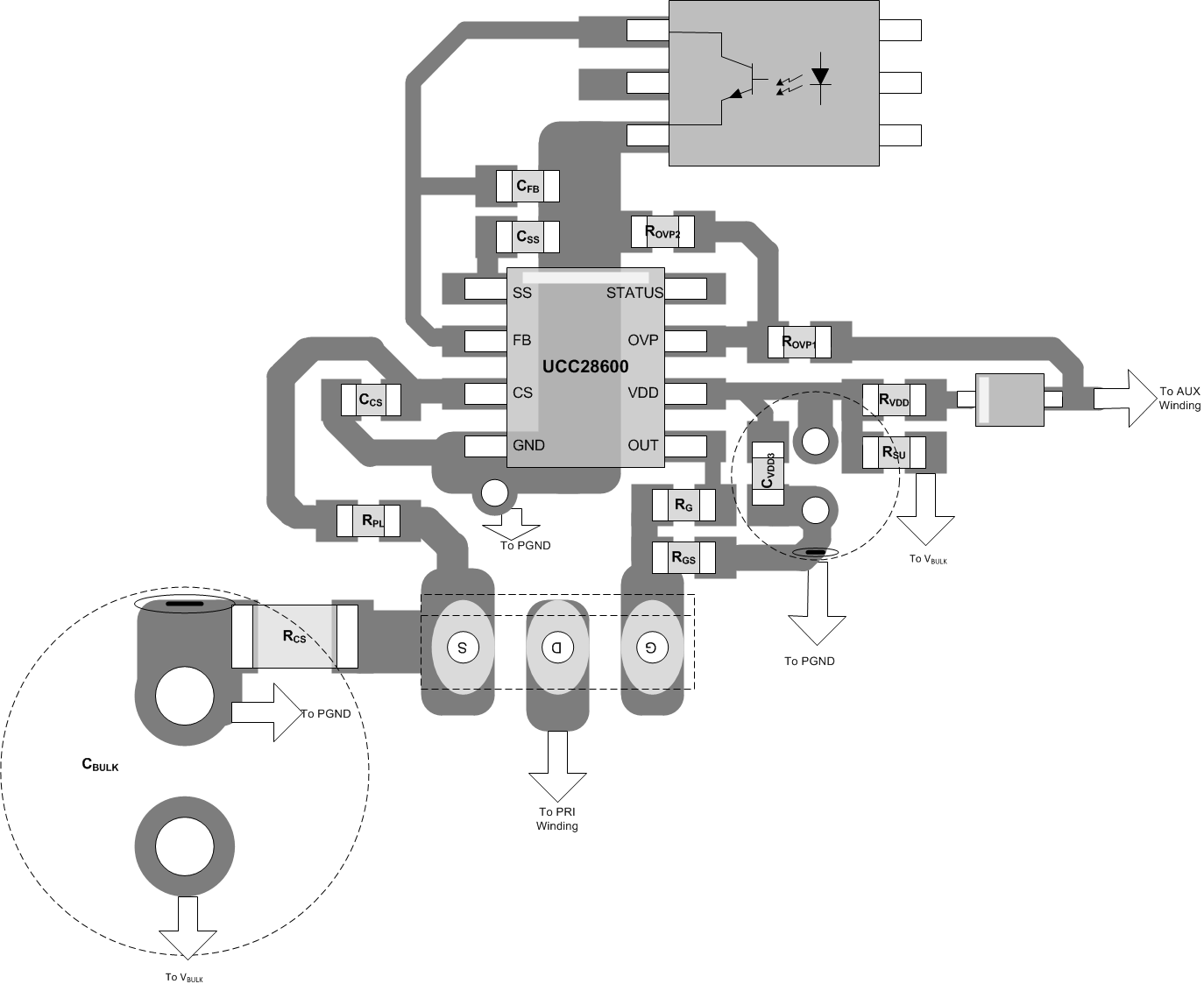
The partial layout example shown in Figure 25 demonstrates an effective component and track arrangement for the printed circuit board. Actual board layout must conform to the constraints on a specific design, so many variations are possible.
 Figure 25. Partial Layout Example Showing Component Placement