SLUS646K November 2005 – August 2015 UCC28600
PRODUCTION DATA.
- 1 Features
- 2 Applications
- 3 Description
- 4 Revision History
- 5 Pin Configuration and Functions
- 6 Specifications
- 7 Detailed Description
- 8 Application and Implementation
- 9 Power Supply Recommendations
- 10Layout
- 11Device and Documentation Support
- 12Mechanical, Packaging, and Orderable Information
8 Application and Implementation
NOTE
Information in the following Applications section is not part of the TI component specification, and TI does not warrant its accuracy or completeness. TI’s customers are responsible for determining suitability of components for their purposes. Customers should validate and test their design implementation to confirm system functionality.
8.1 Application Information
The UCC28600 device is a flyback controller that operates in a mode that is determined by the FB voltage. Line and load conditions set the FB voltage and the controller will operate in Green Mode (GM) under light-load conditions, Frequency Foldback Mode (FFM) when operating at loads approximately between 10% and 30% full rated load, and Quasi-Resonant (QR) or Discontinuous Mode (DCM) at higher loads. Valley switching under all modes, except green mode, reduces switching losses and improves efficiency. Valley skipping also helps reduce EMI. A dedicated STATUS pin is used in higher power applications that use a power factor corrected (PFC) front end. Under light-load conditions, the STATUS signal can be used to disconnect the bias power to the PFC controller, reducing light-load power consumption.
8.2 Typical Application
A typical application for the UCC28600 is an off-line flyback controller from 65 W to 120 W, using a PFC output voltage as its input, as shown in Figure 13. The PFC stage is assumed to operate from a universal AC input and can be controlled by a device such as the UCC28051. The auxiliary winding provides the bias to the controllers and provides over voltage protection and valley switching information, as well as bias to the UCC28600 and UCC28051. The UCC28600 will disable the PFC controller during green mode operation, improving light-load system efficiency. The series resistor connected between the current sense pin and the current sense resistor programs the power limit of the converter. Low valley voltage switching and multi-mode operation will keep the efficiency curve high over the entire operation range. Typical applications include bias supplies for LCD monitors, LCD and PDP televisions, set top boxes, AC-DC adaptors, and energy efficient power supplies up to 200 W.
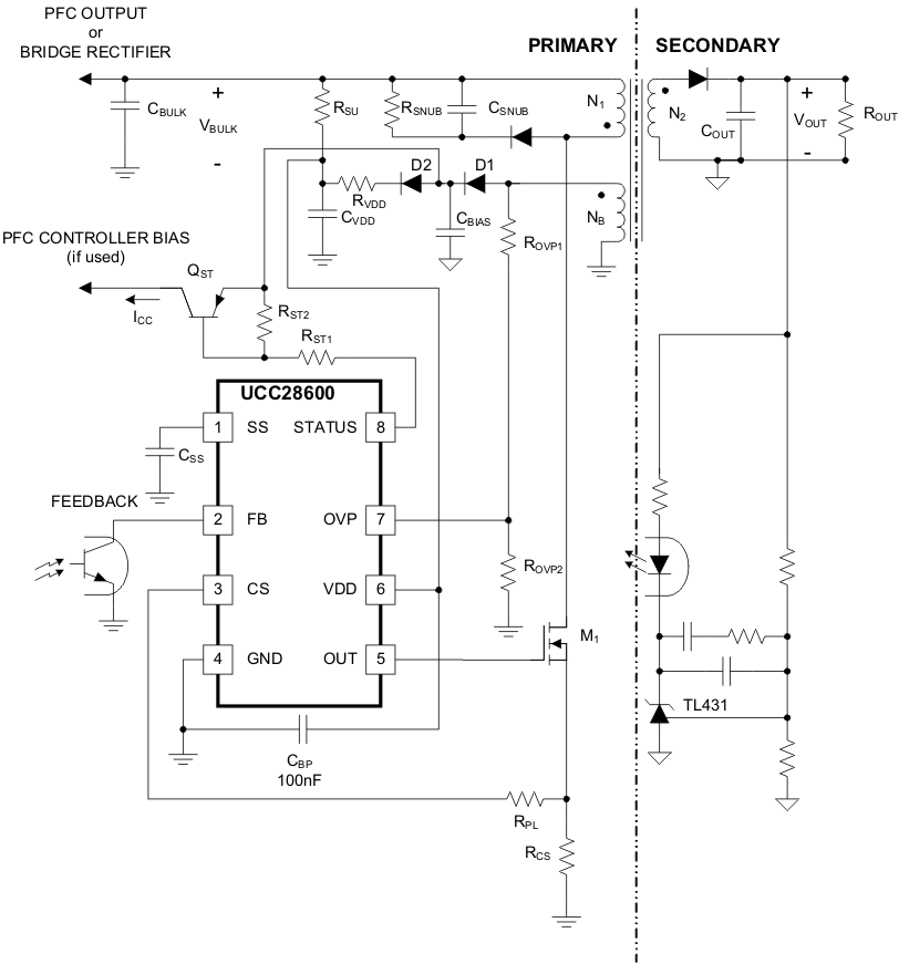 Figure 13. Simplified Application
8.2.1 Design Requirements
The following table illustrates a typical set of performance requirements for an off-line flyback converter.
Table 2. Design Example Performance Requirements
| PARAMETER | CONDITIONS | MIN | NOM | MAX | UNIT | |
|---|---|---|---|---|---|---|
| VIN | AC line input voltage | Input to PFC stage | 85 | 115/230 | 265 | VRMS |
| fLINE | Line frequency | 47 | 50/60 | 63 | Hz | |
| PFCOUTPUT | PFC output voltage | 350 | 390 | 400 | V | |
| PFC | Input power factor | VIN = 115 VRMS, IOUT = 6.2 A | 0.998 | |||
| VIN = 230 VRMS, IOUT = 6.2 A | 0.97 | |||||
| VOUT | Output voltage | 85 VRMS ≤ VIN ≤ 265 VRMS, 0 A ≤ IOUT ≤ 6.2 A |
19.0 | 19.4 | 19.8 | V |
| IOUT | Output load current | 85 VRMS ≤ VIN ≤ 265 VRMS | 0 | 6.2 | A | |
| VRIPPLE | Output voltage ripple | 85 VRMS ≤ VIN ≤ 265 VRMS, IOUT = 6.2 A |
250 | mV | ||
| VOVP | Output over voltage limit | VIN = 115 VRMS, IOUT = 6.2 A | 23.4 | V | ||
| VIN = 230 VRMS, IOUT = 6.2 A | 23.6 | V | ||||
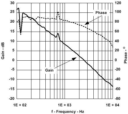
| fCO | Control loop bandwidth | VIN = 115 VRMS, IOUT = 3 A | 2.6 | kHz | ||
| Phase margin | VIN = 115 VRMS, IOUT = 3 A | 70 | degrees | |||
| ηPEAK | Peak efficiency | VIN = 265 VRMS, IOUT = 6 A | 87.4% | |||
| η | Full load efficiency | VIN = 115 VRMS, IOUT = 6.2 A | 82.7% | |||
| VIN = 230 VRMS, IOUT = 6.2 A | 86.4% | |||||
| No load power consumption | VIN = 115 VRMS, IOUT = 0 A | 230 | mW | |||
| VIN = 230 VRMS, IOUT = 0 A | 420 | mW | ||||
8.2.2 Detailed Design Procedure
This procedure outlines the steps to design an off-line universal input quasi-resonant flyback converter using the UCC28600. Refer to Figure 13 for component names and network locations. For additional design help, the design calculator, SLVC104, provides a user-interactive iterative process for selecting recommended component values for an optimum design when used without a PFC input.
8.2.2.1 Input Bulk Capacitor and Minimum Bulk Voltage
Bulk capacitance may consist of one or more capacitors connected in parallel, often with some inductance between them to suppress differential-mode conducted noise. EMI filter design is beyond the scope of this design procedure.
The minimum bulk valley voltage, VBULK(min) is dependent upon the input CBULK capacitor value; this minimum valley voltage is used in the power stage design. The input capacitor is chosen to maintain an acceptable input voltage ripple. For a design that uses a regulated PFC output voltage for the input rail the required input capacitor to the flyback stage is calculated using the minimum PFC output voltage, VPFCoutput(min). Assuming a 15% ripple, the desired minimum bulk valley voltage is:
Designs that do not have a PFC input stage will require a much larger input capacitor. The VBULK(min) when designing without a PFC input stage will be based upon the allowable voltage at the valley of the ripple on the input rail, which can be 25% to 40% of the minimum rectified AC line voltage. Under those conditions, substitute the value of the minimum rectified line voltage for VPFCoutput(min) and the value of the maximum rectified line voltage wherever VPFCoutput(max) is used.
The maximum input power, PIN, is estimated by the output power, POUT, and full-load efficiency target, η, as shown:

The following equation provides an accurate solution for determining the input capacitance needed to achieve the minimum bulk valley voltage target, VBULK(min):

If an input capacitance other than the calculated value is used, iterate the VBULK(min) value until the desired capacitance is obtained so that the actual VBULK(min) is determined.
8.2.2.2 Transformer Turns Ratio and Primary Inductance
The allowable flyback voltage, VFLYBACK, seen by the MOSFET, determines the minimum primary to secondary turns-ratio, NPS. The flyback voltage is calculated based upon the acceptable Drain to Source voltage rating of the MOSFET and the maximum PFC output voltage rail, VPFCoutput(max) (or rectified maximum line voltage if not using a PFC input stage), and derating to account for voltage spikes due to leakage inductance:

Typically, in an off-line design or a design with a PFC output voltage of 390 VDC to 400 VDC, a MOSFET rated for VDS(max) of 600 VDS or greater is used. The primary to secondary turns-ratio takes the output diode voltage drop, VF, into account:

The primary to bias winding turns ratio is calculated, based upon the desired bias voltage, VBIAS, for the UCC28600 controller and the PFC controller bias voltage, making sure to avoid the absolute maximum rating for VDD of each controller:

The switching frequency at the minimum bulk valley voltage is used as a limiting factor for the maximum primary inductance. The UCC28600 will operate in quasi-resonant mode during operation at maximum load, minimum input voltage and its peak primary current and its switching frequency will be modulated during each switching cycle. Using a switching frequency of 80 kHz, for fSW, at this operating point will give adequate margin for manufacturing tolerances in the transformer, the parasitic switch node capacitance, which influences the resonant frequency to each valley, and keep the controller from trying to go continuous during transient conditions. The switching period, tSW, is equal to 1/fSW. Using volt-second balance, the maximum primary inductance can be calculated:

The resistor divider on OVP senses the line voltage during the switch on-time when the auxiliary winding voltage is proportional to the line voltage. During this portion of the switching cycle, the OVP pin is internally clamped to approximately 0 V and sources current proportional to the line voltage. The ROVP1 resistor is chosen using the nominal line over-voltage protection current threshold, IOVP(line), which is equal to 450 µA.

The OVP pin is also used to sense the output voltage when the OUT signal is low. To set the output over-voltage level, VOUT(shutdown), which is the desired voltage level on the output that would cause the controller to shutdown, use the load overvoltage protection threshold, VOVP(load), equal to 3.75 V, to determine the required ROVP2 resistor.

The peak primary current at low input voltage, full load, IP(1), can be estimated with the following equation:

The switching frequency at maximum input voltage can be estimated:

Now that the switching frequency at the maximum input voltage has been determined, the peak primary current at maximum load, IP(2), at the maximum input voltage can be calculated:

The power limit current that is sourced at the CS pin adds a voltage step to the CS waveform that is proportional to the line voltage. At minimum input voltage, maximum load, this current is referred to as ICS(1) and can be estimated from the following equation:

At maximum input voltage and maximum load, the power limit current sourced from CS is referred to as ICS(2) and is estimated using the same formula:

The appropriate values of the current sense resistor, RCS, and the power limit resistor, RPL, are both dependent upon the internal power limit threshold, VPL = 1.20 V, the CS offset voltage, VCS(os) = 0.40 V, peak primary currents, and the power limit currents, calculated above, and can be calculated as shown:


8.2.2.3 Non-Ideal Current Sense Value
Resistors RCS, RPL, ROVP1 and ROVP2 must be programmed as a set due to functional interactions in the converter. Often, the ideal value for RCS is not available because the selection range of current sense resistors is too coarse to meet the required power limit tolerances. This issue can be solved by using the next larger available value of RCS and use a resistive divider with a Thevenin resistance that is equal to the ideal RPL value in order to attenuate the CS signal to its ideal value, as shown in Figure 14. The equations for modifying the circuit are:

where
- RDCS = ideal, but non-standard, value of current sense resistor.
- RPL = previously calculated value of the power limit resistor.

where
- RCS = available, standard value current sense resistor.
The board should be laid out to include RPL2 in order to fascillitate final optimization of the design based upon readily available components.
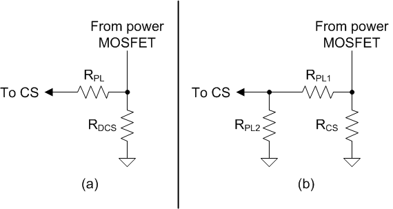 Figure 14. Modifications to Fit a Standard Current Sense Resistor Value
8.2.2.4 Snubber Damping
Resonance between the leakage inductance and the MOSFET drain capacitance can cause false load-OVP faults, in spite of the typical 2-μs delay in load-OVP detection. The bias winding is sensitive to the overshoot and ringing because it is well coupled to the primary winding. A technique to eliminate the problem is to use an R2CD snubber instead of an RCD snubber, shown in Figure 15. A damping resistor added to the RCD snubber reduces ringing between the drain capacitor and the inductance when the snubber diode commutates OFF.
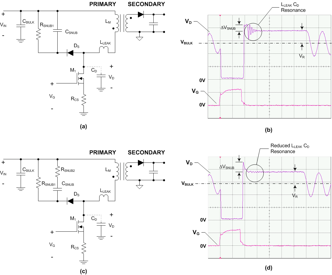 Figure 15. (a) RCD Snubber, (b) RCD Snubber Waveform, (c) R2CD Snubber, (d) R2CD Snubber Waveform
Begin the design of the R2CD using the same procedure as designing an RCD snubber. Then, add the damping resistor, RSNUB2. The procedure is as follows:

Select a capacitor for ΔVSNUB:

Pick RSNUB to discharge CSNUB:

Pick RSNUB2 to dampen the LLEAK-CSNUB resonance with a Q that is between 1.7 and 2.2:


For the original selection of ΔVSNUB,

8.2.2.5 Open Loop Test Circuit
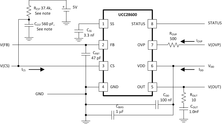 Figure 16. Open Loop Test Circuit
NOTE
RCST and CCST are not connected for maximum and minimum duty cycle tests, current sense tests and power limit tests.
8.2.3 Application Curves
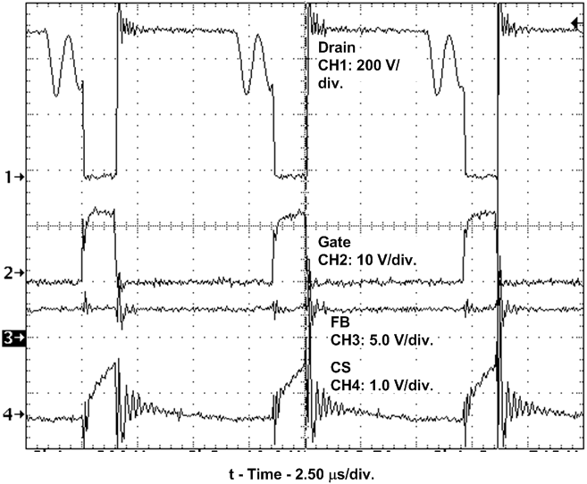
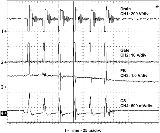
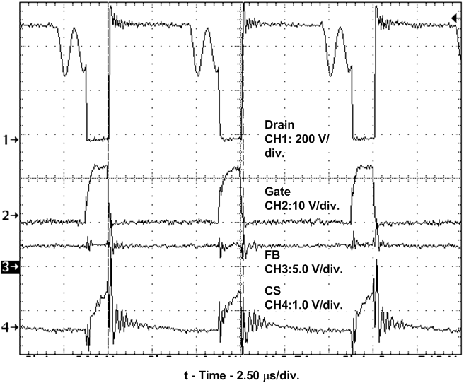
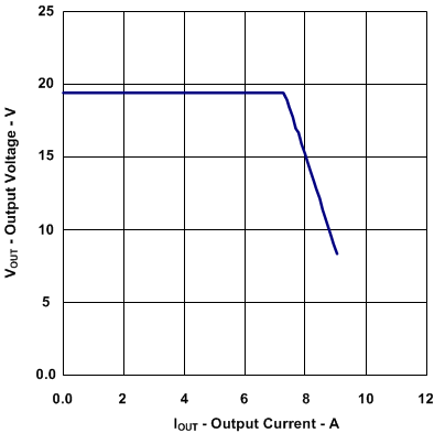
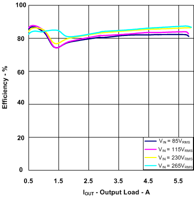
The following figures show the UCC28600 in various operating modes in a 120-W converter, output voltage equal to 19.4 V.
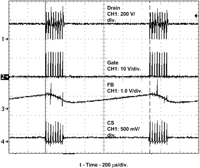
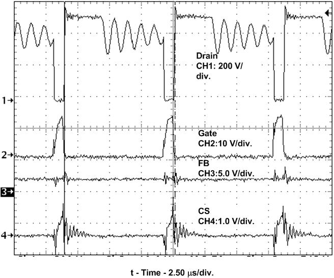
90% Full-Rated Load
74% Full-Rated Load
8.3 Do's and Don'ts
Always be sure to do the following:
- Isolate the STATUS pin from the start up resistor with a diode to prevent the bias current from the bulk input rail from being diverter away from VDD and into STATUS circuit.
- Use a bypass capacitor on VDD, minimum value of 0.1 µF, to filter high frequency noise.
- Use a large bulk capacitor on VDD to hold the bias above the UVLO turn off threshold between the long periods of time between burst packets at light load.
- Use a large enough capacitor on SS to prevent triggering power limit when charging the output capacitor bank at turn on.
- Place the SS capacitor as close as possible to the SS pin with short traces and return to the quiet signal ground.
- Design the loop crossover frequency to be between 2 kHz to 3 kHz at nominal input voltage and 50% load with a phase margin of 70 degrees to satisfactorily stabilize the loop for the entire range of operation.
- Add a small filter capacitor to CS to effectively create an RC low pass filter in conjunction with the power limit resistor, RPL, which will improve noise immunity at the current sense pin.
- Place a 10-kΩ resistor between the gate of the MOSFET and ground to discharge the gate capacitance and protect against inadvertent dv/dt triggered turn-on.
- Use a small value gate drive resistor in series with the gate drive to control the turn on transition time and reduce the dv/dt ringing in this node.
- Select the ROVP1, ROVP2, RPL, and RCS together as the OVP resistors set up an internal dependent current source that impact the RCS and RPL component values.
- Design the transformer so the bias winding is well coupled to both the primary winding and the secondary winding. The bias winding is used not only for VDD bias but also for valley detection, line over-voltage, load over-voltage, and power limit off-set current.
CAUTION
Do not use a filter capacitor larger than 390 pF on the FB pin, this capacitor will provide a delay time to over-load response; capacitors larger than 390 pF will adversely affect performance.
