ZHCS446A September 2011 – December 2014 UCC28063
PRODUCTION DATA.
- 1 特性
- 2 应用
- 3 说明
- 4 修订历史记录
- 5 说明(继续)
- 6 Pin Configuration and Functions
- 7 Specifications
-
8 Detailed Description
- 8.1 Overview
- 8.2 Functional Block Diagram
- 8.3
Feature Description
- 8.3.1 Principles of Operation
- 8.3.2 Natural Interleaving
- 8.3.3 On-Time Control, Maximum Frequency Limiting, and Restart Timer
- 8.3.4 Distortion Reduction
- 8.3.5 Zero-Current Detection and Valley Switching
- 8.3.6 Phase Management and Light-Load Operation
- 8.3.7 External Disable
- 8.3.8 Improved Error Amplifier
- 8.3.9 Soft Start
- 8.3.10 Brownout Protection
- 8.3.11 Dropout Detection
- 8.3.12 VREF
- 8.3.13 VCC
- 8.3.14 Control of Downstream Converter
- 8.3.15
System Level Protections
- 8.3.15.1 Failsafe OVP - Output Overvoltage Protection
- 8.3.15.2 Overcurrent Protection
- 8.3.15.3 Open-Loop Protection
- 8.3.15.4 VCC Undervoltage Lock-Out (UVLO) Protection
- 8.3.15.5 Phase-Fail Protection
- 8.3.15.6 CS-Open, TSET-Open and -Short Protection
- 8.3.15.7 Thermal Shutdown Protection
- 8.3.15.8 AC-Line Brownout and Dropout Protections
- 8.3.15.9 Fault Logic Diagram
- 8.4 Device Functional Modes
-
9 Applications and Implementation
- 9.1 Application Information
- 9.2
Typical Application
- 9.2.1 Design Requirements
- 9.2.2
Detailed Design Procedure
- 9.2.2.1 Inductor Selection
- 9.2.2.2 ZCD Resistor Selection (RZA, RZB)
- 9.2.2.3 HVSEN
- 9.2.2.4 Output Capacitor Selection
- 9.2.2.5 Selecting (RS) For Peak Current Limiting
- 9.2.2.6 Power Semiconductor Selection (Q1, Q2, D1, D2)
- 9.2.2.7 Brownout Protection
- 9.2.2.8 Converter Timing
- 9.2.2.9 Programming VOUT
- 9.2.2.10 Voltage Loop Compensation
- 9.2.3 Application Curves
- 10Power Supply Recommendations
- 11Layout
- 12器件和文档支持
- 13机械、封装和可订购信息
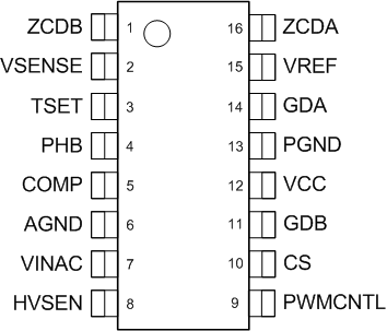
6 Pin Configuration and Functions
D Package
16-Pin SOIC
Top View

Pin Functions
| PIN | I/O | DESCRIPTION | |
|---|---|---|---|
| NAME | NO. | ||
| AGND | 6 | - | Analog Ground |
| COMP | 5 | O | Error Amplifier Output |
| CS | 10 | I | Current Sense Input |
| GDA | 14 | O | Channel A and Channel B Gate Drive Output |
| GDB | 11 | O | |
| HVSEN | 8 | I | High Voltage Output Sense |
| PHB | 4 | I | Phase-B Enable/Disable |
| PWMCNTL | 9 | O | PWM-Control Output |
| TSET | 3 | I | Timing Set |
| VCC | 12 | - | Bias Supply Input |
| VINAC | 7 | I | Input AC Voltage Sense |
| VREF | 15 | O | Voltage Reference Output |
| VSENSE | 2 | I | Output DC Voltage Sense |
| ZCDA | 16 | I | Zero Current Detection Inputs |
| ZCDB | 1 | I | |