SLUS515G September 2002 – December 2015 UCC28050 , UCC28051 , UCC38050 , UCC38051
PRODUCTION DATA.
- 1 Features
- 2 Applications
- 3 Description
- 4 Revision History
- 5 Pin Configuration and Functions
- 6 Specifications
- 7 Detailed Description
- 8 Application and Implementation
- 9 Power Supply Recommendations
- 10Layout
- 11Device and Documentation Support
- 12Mechanical, Packaging, and Orderable Information
7 Detailed Description
7.1 Overview
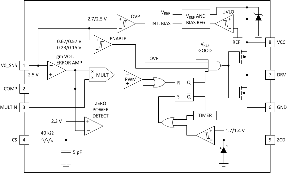
The UCC38050 and UCC38051 are PFC controllers for low-to-medium power applications requiring compliance with IEC 1000-3-2 harmonic reduction. The controller is designed for a boost preregulator operating in transition mode (also referred to as boundary-conduction mode or critical conduction-mode operation). It features a transconductance voltage amplifier for feedback error processing, a simple multiplier for generating a current command proportional to the input voltage, a current-sense (PWM) comparator, PWM logic, and a totem-pole driver for driving an external FET.
The UCC38050 and UCC38051, while being pin-compatible with other industry controllers providing similar functionality, offer many feature enhancements and tighter specifications, leading to an overall reduction in system implementation cost. The system performance is enhanced by incorporation of a zero-power detect function, which allows the controller output to shut down at light load conditions without running into overvoltage. The device also features innovative slew rate enhancement circuits, which improve the large signal transient performance of the voltage error amplifier. The low start-up and operating currents of the device result in low power consumption and ease of start-up. Highly accurate internal bandgap reference leads to tight regulation of output voltage in normal and OVP conditions, resulting in higher system reliability. The enable comparator ensures that the controller is off if the feedback sense path is broken or if the input voltage is very low.
There are two key parameteric differences between UCC38050 and UCC38051. The UVLO turn-on threshold of UCC38050 is 15.8 V, while for UCC38051 it is 12.5 V. Secondly, the gM amplifier source current for UCC38050 is typically 1.3 mA, while for UCC38051 it is 300 μA. The higher UVLO turn-on threshold of the UCC38050 allows quicker and easier start-up with a smaller VCC capacitance, while the lower UVLO turn-on threshold of UCC38051 allows the operation of the PFC chip to be easily controlled by the downsteam PWM controller in two-stage power converters. The UCC38050 gM amplifier also provides a full 1.3-mA typical source current for faster start-up and improved transient response when output is low, either at start-up or during transient conditions. The UCC38051 scales this source current back down to 300-μA typical source current to gradually increase the error voltage, preventing a step increase in line currents at start-up, but still providing good transient response. The UCC38051 is suitable for multiple applications, including AC adapters, where a two-stage power conversion is needed. The UCC38050 is suitable for applications such as electronic ballasts, where there is no down-stream PWM conversion and the advantages of a smaller VCC capacitor and improved transient response can be realized.
7.2 Functional Block Diagram

7.3 Feature Description
7.3.1 UVLO and Reference Block
This block generates a precision reference voltage used to obtain tightly controlled UVLO threshold. In addition to generating a 2.5-V reference for the non-inverting terminal of the gM amplifier, it generates the reference voltages for blocks such as OVP, enable, zero power, and multiplier. An internal rail of 7.5 V is also generated, to drive all the internal blocks.
7.3.2 Error Amplifier
The voltage error amplifier in UCC3805x is a transcoductance amplifier, with a typical transconductance value of 90 μS. A transconductance amplifier is advantageous in that the inverting input of the amplifier is solely determined by the external resistive-divider from the output voltage, and not the transient behavior of the amplifier itself. This allows the VO_SNS pin to be used for sensing overvoltage conditions.
The sink and source capability of the error amplifier is approximately 10 μA during normal operation of the amplifier. However, when the VO_SNS pin voltage is beyond the normal operating conditions (VO_SNS > 1.05 × VREF, VO_SNS < 0.88 × VREF), additional circuitry to enhance the slew-rate of the amplifier is activated. Enhanced slew-rate of the compensation capacitor results in a faster start-up and transient response. This prevents the output voltage from drifting too high or too low, which can happen if the compensation capacitor were to be slewed by the normal slewing current of 10 μA. When VO_SNS rises above the normal range, the enhanced sink current capability is in excess of 1 mA. When VO_SNS falls below the normal range, the UCC38050 can source more than 1 mA, and the UCC38051 sources approximately 300 μA. The limited source current in the UCC38051 helps to gradually increase the error voltage on the COMP pin preventing a step increase in line current. The actual rate of increase of VCOMP depends on the compensation network connected to the COMP pin.
7.3.3 Zero Current Detection and Re-Start Timer Blocks
When the boost inductor current becomes zero, the voltage at the power MOSFET drain end falls. This is indirectly sensed with a secondary winding connected to the ZCD pin. The internal active clamp circuitry prevents the voltage from going to a negative or a high positive value. The clamp has the sink and source capability of 10 mA. The resistor value in series with the secondary winding should be chosen to limit the ZCD current to less than 10 mA. The rising edge threshold of the ZCD comparator can be as high as 2 V. The auxiliary winding should be chosen such that the positive voltage (when the power MOSFET is off) at the ZCD pin is in excess of 2 V.
The restart timer attempts to set the gate drive high in case the gate drive remains off for more than 400 μs nominally. The minimum guaranteed time period of the timer is 200 μs. This translates to a minimum switching frequency of 5 kHz. In other words, the boost inductor value should be chosen for switching frequencies greater than 5 kHz.
7.3.4 Enable Block
The gate drive signal is held low if the voltage at the VO_SNS pin is less than the ENABLE threshold. This feature can disable the converter by pulling VO_SNS low. If the output feedback path is broken, VO_SNS is pulled to ground, and the output is disabled to protect the power stage.
7.3.5 Zero Power Block
When the output of the gM amplifier goes below 2.3 V, the zero power comparator latches the gate drive signal low. The slew rate enhancement circuitry of the gM amplifier activated during overvoltage conditions slews the COMP pin to approximately 2.4 V. This ensures that the zero power comparator is not activated during transient behavior, when the slew rate enhancement circuitry is enhanced.
7.3.6 Multiplier Block
The multiplier block has two inputs. One is the error amplifier output voltage (VCOMP), and the other is VMULTIN, which is obtained by a resistive divider from the rectified line. The multiplier output is approximately 0.67 × VMULTIN × (VCOMP − 2.5 V). There is a positive offset of about 75 mV to the VMULTIN signal because this improves the zero-crossing distortion and thus the THD performance of the controller in the application. The dynamic range of the inputs can be found in Electrical Characteristics.
7.3.7 Overvoltage Protection (OVP) Block
The OVP feature in the part is not activated under most operating conditions because of the presence of the slew rate enhancement circuitry present in the error amplifier. As soon as the output voltage reaches to approximately 5% to 7% above the nominal value, the slew rate enhancement circuit is activated, and the error amplifier output voltage is pulled below the dynamic range of the multiplier block. This prevents further rise in output voltage.
If the COMP pin is not pulled low fast enough and the voltage rises further, the OVP circuit acts as a second line of protection. When the voltage at the VO_SNS pin is more than 7.5% of the nominal value (> (VREF + 0.19)), the OVP feature is activated. It stops the gate drive from switching as long as the voltage at the VO_SNS pin is above the nominal value (VREF). This prevents the output DC voltage from going above 7.5% of the nominal value designed for, and protects the switch and other components of the system such as the boost capacitor.
7.4 Device Functional Modes
7.4.1 Transition Mode Control
The boost converter, the most common topology used for power factor correction, can operate in two modes: continuous conduction code (CCM) and discontinuous conduction mode (DCM). Transition mode control, also referred to as critical conduction mode (CRM) or boundary conduction mode, maintains the converter at the boundary between CCM and DCM by adjusting the switching frequency.
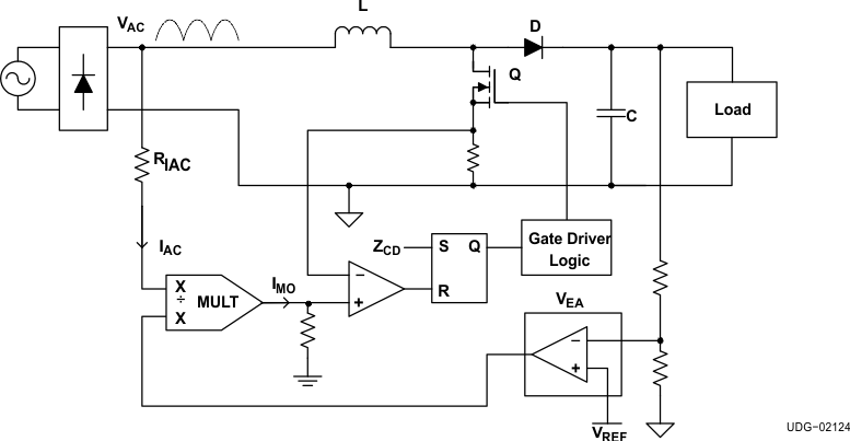
The CRM converter typically uses a variation of hysteretic control, with the lower boundary equal to zero current. It is a variable frequency control technique that has inherently stable input current control while eliminating reverse recovery rectifier losses. As shown in Figure 17, the switch current is compared to the reference signal (output of the multiplier) directly. This control method has the advantage of simple implementation and good power factor correction.
 Figure 17. Basic Block Diagram of CRM Boost PFC
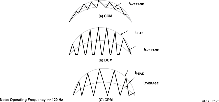
The power stage equations and the transfer functions of the CRM are the same as the CCM. However, implementations of the control functions are different. Transition mode forces the inductor current to operate just at the border of CCM and DCM. The current profile is also different, and affects the component power loss and filtering requirements. The peak current in the CRM boost is twice the amplitude of CCM, leading to higher conduction losses. The peak-to-peak ripple is twice the average current, which affects MOSFET switching losses and magnetics ac losses.
 Figure 18. PFC Inductor Current Profiles
For low to medium power applications up to approximately 300 W, the CRM boost has an advantage in losses. The filtering requirement is not severe, and therefore is not a disadvantage. For medium to higher power applications, where the input filter requirements dominate the size of the magnetics, the CCM boost is a good choice due to lower peak currents (which reduces conduction losses) and lower ripple current (which reduces filter requirements). The main tradeoff in using CRM boost is lower losses due to no reverse recovery in the boost diode vs. higher ripple and peak currents.