SLUS846C September   2008  – June 2015 UCC25600

PRODUCTION DATA.  

  1. Features
  2. Applications
  3. Description
  4. Revision History
  5. Pin Configuration and Functions
  6. Specifications
    1. 6.1 Absolute Maximum Ratings
    2. 6.2 ESD Ratings
    3. 6.3 Recommended Operating Conditions
    4. 6.4 Thermal Information
    5. 6.5 Electrical Characteristics
    6. 6.6 Typical Characteristics
  7. Detailed Description
    1. 7.1 Overview
    2. 7.2 Functional Block Diagram
    3. 7.3 Feature Description
      1. 7.3.1 Soft Start
      2. 7.3.2 Overcurrent Protection
      3. 7.3.3 Gate Driver
      4. 7.3.4 Overtemperature Protection
    4. 7.4 Device Functional Modes
      1. 7.4.1 Burst-Mode Operation
      2. 7.4.2 VCC
  8. Application and Implementation
    1. 8.1 Application Information
      1. 8.1.1 Principal of Operation
      2. 8.1.2 Adjustable Dead Time
      3. 8.1.3 Oscillator
    2. 8.2 Typical Application
      1. 8.2.1 Design Requirements
      2. 8.2.2 Detailed Design Procedure
      3. 8.2.3 Application Curves
  9. Power Supply Recommendations
  10. 10Layout
    1. 10.1 Layout Guidelines
    2. 10.2 Layout Example
  11. 11Device and Documentation Support
    1. 11.1 Community Resources
    2. 11.2 Trademarks
    3. 11.3 Electrostatic Discharge Caution
    4. 11.4 Glossary
  12. 12Mechanical, Packaging, and Orderable Information

封装选项

机械数据 (封装 | 引脚)
散热焊盘机械数据 (封装 | 引脚)
订购信息

10 Layout

10.1 Layout Guidelines

Four-layer layout is recommended

A 1-µF ceramic decoupling capacitor is recommended, to be placed as close as possible between the VCC terminal and GND, and tracked directly to both terminals.

Place CSS, RDT, Rp, Cp, RT1, and RT2 as close as possible to the UCC25600.

Connect a regulated bias supply to the VCC pin.

10.2 Layout Example
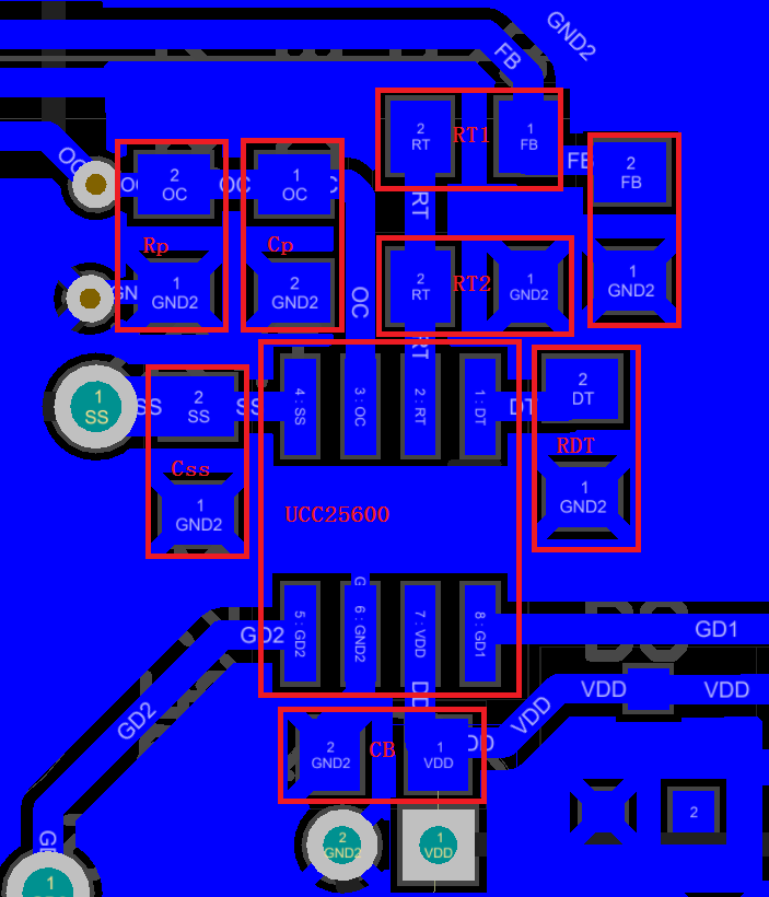
UCC25600 slus846_layout.pngFigure 27. Board Layout Example