SCDS285B March 2009 – August 2016 TS5A21366
PRODUCTION DATA.
- 1 Features
- 2 Applications
- 3 Description
- 4 Revision History
- 5 Pin Configuration and Functions
-
6 Specifications
- 6.1 Absolute Maximum Ratings
- 6.2 ESD Ratings
- 6.3 Recommended Operating Conditions
- 6.4 Thermal Information
- 6.5 Electrical Characteristics for 5-V Supply
- 6.6 Electrical Characteristics for 3.3-V Supply
- 6.7 Electrical Characteristics for 2.5-V Supply
- 6.8 Electrical Characteristics for 1.8-V Supply
- 6.9 Typical Characteristics
- 7 Parameter Measurement Information
- 8 Detailed Description
- 9 Application and Implementation
- 10Power Supply Recommendations
- 11Layout
- 12Device and Documentation Support
- 13Mechanical, Packaging, and Orderable Information
7 Parameter Measurement Information
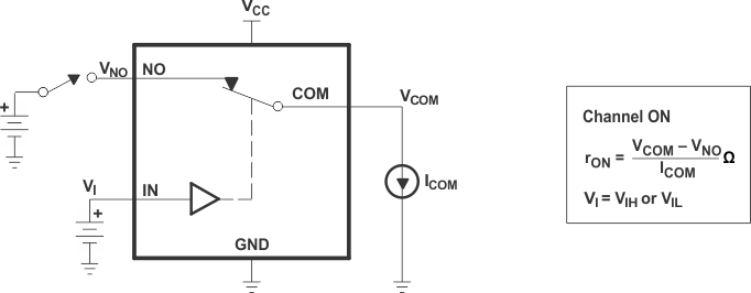 Figure 15. ON-State Resistance (rON)
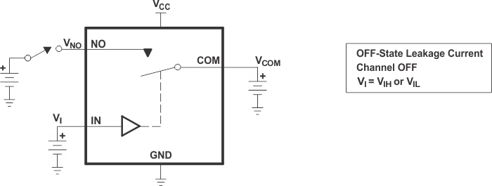 Figure 16. OFF-State Leakage Current (ICOM(OFF), INO(OFF), ICOM(PWROFF), INOC(PWR(FF))
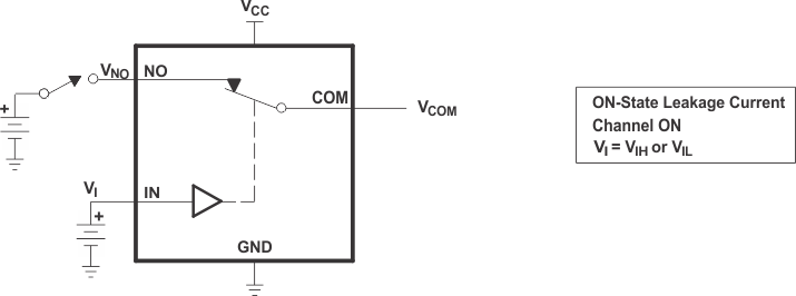 Figure 17. ON-State Leakage Current (ICOM(ON), INO(ON))
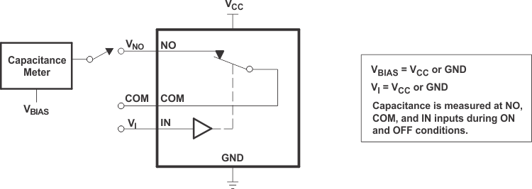 Figure 18. Capacitance (CI, CCOM(OFF), CCOM(ON), CNO(OFF), CNO(ON))
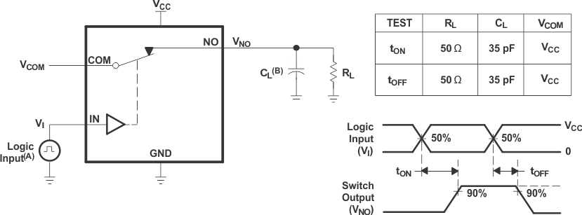
A. All input pulses are supplied by generators having the following characteristics: PRR ≤ 10 MHz, ZO = 50 Ω, tr ≤ 5 ns, tf ≤ 5 ns.
B. CL includes probe and jig capacitance.
Figure 19. Turnon (tON) and Turnoff Time (tOFF)
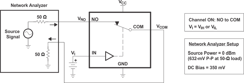 Figure 20. Bandwidth (BW)
 Figure 21. OFF Isolation (OISO)
 Figure 22. Crosstalk (XTALK)

A. CL includes probe and jig capacitance.
B. All input pulses are supplied by generators having the following characteristics: PRR ≤ 10 MHz, ZO = 50 Ω, tr ≤ 5 ns,
tf ≤ 5 ns.
Figure 23. Charge Injection (QC)
tf ≤ 5 ns.
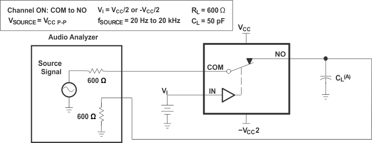
A. CL includes probe and jig capacitance.
Figure 24. Total Harmonic Distortion (THD+N)
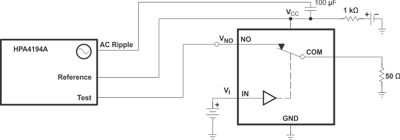 Figure 25. Power Supply Rejection Ratio (PSRR)
Table 1. Parameter Description
| SYMBOL | DESCRIPTION |
|---|---|
| VCOM | Voltage at COM |
| VNO | Voltage at NO |
| ron | Resistance between COM and NO ports when the channel is ON |
| ron(flat) | Difference between the maximum and minimum value of ron in a channel over the specified range of conditions |
| INO(OFF) | Leakage current measured at the NO port, with the corresponding channel (NO to COM) in the OFF state |
| INO(ON) | Leakage current measured at the NO port, with the corresponding channel (NO to COM) in the ON state and the output (COM) open |
| ICOM(OFF) | Leakage current measured at the COM port, with the corresponding channel (COM to NO) in the OFF state |
| ICOM(ON) | Leakage current measured at the COM port, with the corresponding channel (COM to NO) in the ON state and the output (NO) open |
| VIH | Minimum input voltage for logic high for the control input (IN) |
| VIL | Maximum input voltage for logic low for the control input (IN) |
| VI | Voltage at the control input (IN) |
| IIH, IIL | Leakage current measured at the control input (IN) |
| tON | Turnon time for the switch. This parameter is measured under the specified range of conditions and by the propagation delay between the digital control (IN) signal and analog output (COM or NO) signal when the switch is turning ON. |
| tOFF | Turnoff time for the switch. This parameter is measured under the specified range of conditions and by the propagation delay between the digital control (IN) signal and analog output (COM or NO) signal when the switch is turning OFF. |
| QC | Charge injection is a measurement of unwanted signal coupling from the control (IN) input to the analog (NO or COM) output. This is measured in coulomb (C) and measured by the total charge induced due to switching of the control input. Charge injection, QC = CL × ΔVCOM, CL is the load capacitance and ΔVCOM is the change in analog output voltage. |
| CNO(OFF) | Capacitance at the NO port when the corresponding channel (NO to COM) is OFF |
| CNO(ON) | Capacitance at the NO port when the corresponding channel (NO to COM) is ON |
| CCOM(OFF) | Capacitance at the COM port when the corresponding channel (COM to NO) is OFF |
| CCOM(ON) | Capacitance at the COM port when the corresponding channel (COM to NO) is ON |
| CI | Capacitance of control input (IN) |
| OISO | OFF isolation of the switch is a measurement of OFF-state switch impedance. This is measured in dB in a specific frequency, with the corresponding channel (NO to COM) in the OFF state. |
| XTALK | Crosstalk is a measurement of unwanted signal coupling from an ON channel to an OFF channel (NO1 to NO2). This is measured in a specific frequency and in dB. |
| BW | Bandwidth of the switch. This is the frequency in which the gain of an ON channel is –3 dB below the DC gain. |
| THD+N | Total harmonic distortion describes the signal distortion caused by the analog switch. This is defined as the ratio of root mean square (RMS) value of the second, third, and higher harmonic to the absolute magnitude of the fundamental harmonic. |
| ICC | Static power-supply current with the control (IN) pin at VCC or GND |
| ΔICC | This is the increase in ICC for each control (IN) input that is at the specified voltage, rather than at VCC or GND. |