SLVSDD9 March 2017 TPS92692 , TPS92692-Q1
PRODUCTION DATA.
- 1 Features
- 2 Applications
- 3 Description
- 4 Revision History
- 5 Pin Configuration and Functions
- 6 Specifications
-
7 Detailed Description
- 7.1 Overview
- 7.2 Functional Block Diagram
- 7.3
Feature Description
- 7.3.1 Internal Regulator and Undervoltage Lockout (UVLO)
- 7.3.2 Oscillator
- 7.3.3 Spread Spectrum Frequency Modulation
- 7.3.4 Gate Driver
- 7.3.5 Rail-to-Rail Current Sense Amplifier
- 7.3.6 Transconductance Error Amplifier
- 7.3.7 Switch Current Sense
- 7.3.8 Slope Compensation
- 7.3.9 Analog Adjust Input
- 7.3.10 DIM/PWM Input
- 7.3.11 Series P-Channel FET Dimming Gate Driver Output
- 7.3.12 Soft-Start
- 7.3.13 Current Monitor Output
- 7.3.14 Output Overvoltage Protection
- 7.3.15 Output Short-circuit Protection
- 7.3.16 Thermal Protection
- 7.3.17 Fault Indicator (FLT)
- 7.4 Device Functional Modes
-
8 Application and Implementation
- 8.1
Application Information
- 8.1.1 Duty Cycle Considerations
- 8.1.2 Inductor Selection
- 8.1.3 Output Capacitor Selection
- 8.1.4 Input Capacitor Selection
- 8.1.5 Main Power MOSFET Selection
- 8.1.6 Rectifier Diode Selection
- 8.1.7 LED Current Programming
- 8.1.8 Switch Current Sense Resistor
- 8.1.9 Slope Compensation
- 8.1.10 Feedback Compensation
- 8.1.11 Soft-Start
- 8.1.12 Overvoltage and Undervoltage Protection
- 8.1.13 Analog to PWM Dimming Considerations
- 8.1.14 Direct PWM Dimming Considerations
- 8.1.15 Series P-Channel MOSFET Selection
- 8.2
Typical Applications
- 8.2.1
Typical Boost LED Driver
- 8.2.1.1 Design Requirements
- 8.2.1.2
Detailed Design Procedure
- 8.2.1.2.1 Calculating Duty Cycle
- 8.2.1.2.2 Setting Switching Frequency
- 8.2.1.2.3 Setting Dither Modulation Frequency
- 8.2.1.2.4 Inductor Selection
- 8.2.1.2.5 Output Capacitor Selection
- 8.2.1.2.6 Input Capacitor Selection
- 8.2.1.2.7 Main N-Channel MOSFET Selection
- 8.2.1.2.8 Rectifying Diode Selection
- 8.2.1.2.9 Programming LED Current
- 8.2.1.2.10 Setting Switch Current Limit
- 8.2.1.2.11 Programming Slope Compensation
- 8.2.1.2.12 Deriving Compensator Parameters
- 8.2.1.2.13 Setting Start-up Duration
- 8.2.1.2.14 Setting Overvoltage Protection Threshold
- 8.2.1.2.15 Analog-to-PWM Dimming Considerations
- 8.2.1.3 Application Curves
- 8.2.2
Typical Buck-Boost LED Driver
- 8.2.2.1 Design Requirements
- 8.2.2.2
Detailed Design Procedure
- 8.2.2.2.1 Calculating Duty Cycle
- 8.2.2.2.2 Setting Switching Frequency
- 8.2.2.2.3 Setting Dither Modulation Frequency
- 8.2.2.2.4 Inductor Selection
- 8.2.2.2.5 Output Capacitor Selection
- 8.2.2.2.6 Input Capacitor Selection
- 8.2.2.2.7 Main N-Channel MOSFET Selection
- 8.2.2.2.8 Rectifier Diode Selection
- 8.2.2.2.9 Programming LED Current
- 8.2.2.2.10 Setting Switch Current Limit and Slope Compensation
- 8.2.2.2.11 Programming Slope Compensation
- 8.2.2.2.12 Deriving Compensator Parameters
- 8.2.2.2.13 Setting Startup Duration
- 8.2.2.2.14 Setting Overvoltage Protection Threshold
- 8.2.2.2.15 Direct PWM Dimming Consideration
- 8.2.2.3 Application Curves
- 8.2.1
Typical Boost LED Driver
- 8.1
Application Information
- 9 Power Supply Recommendations
- 10Layout
- 11Device and Documentation Support
- 12Mechanical, Packaging, and Orderable Information
7 Detailed Description
7.1 Overview
The TPS92692 and TPS92692-Q1 devices feature all of the functions necessary to implement a compact LED driver based on step-up or step-down power converter topologies. The devices implement a fixed-frequency, peak current mode control technique to achieve constant output current and fast transient response. The integrated low offset, rail-to-rail current sense amplifier provides the flexibility required to power a single string consisting of 1 to 20 series connected LEDs while maintaining better than 4% current accuracy over the operating temperature range. The LED current regulation threshold is set by the analog adjust input, IADJ and can be externally programmed to implement analog dimming with over 15:1 linear dimming range. The high impedance IADJ input simplifies LED current binning and thermal protection.
The TPS92692 and TPS92692-Q1 devices incorporate an internal PWM generator that can be programmed to implement pulse width modulation (PWM) dimming of LED current. The PWM duty cycle can be varied from 0% to 100% by modulating the analog voltage on DIM/PWM input from 1 V to 3 V. The PWM dimming frequency is externally programmable and is set by the capacitor connected to RAMP input. As an alternative, the TPS92692 and TPS92692-Q1 devices can also be configured to implement direct PWM dimming based on the duty cycle of external PWM signal by connecting a 249-kΩ resistor across RAMP pin and GND. The internal PWM signal controls the GATE and PDRV outputs which control the external n-channel switching FET and p-channel dimming FET connected in series with LED string, respectively.
The current monitor output, IMON, reports the instantaneous status of LED current measured by the rail-to-rail current sense amplifier. This feature indicates instantaneous current as a result of LED short circuit and cable harness failure, independent of LED driver topology. An open-drain fault indicator is also provided to report faults including cycle-by-cycle current limit, output overvoltage, and output undervoltage conditions. LED driver protection with auto-restart (hiccup) mode is enabled by connecting the fault pin (FLT) to the SS pin. Other protection features include VCC undervoltage protection and thermal shutdown. A remote signal can force the device in to shutdown by pulling down on the SS pin.
7.2 Functional Block Diagram
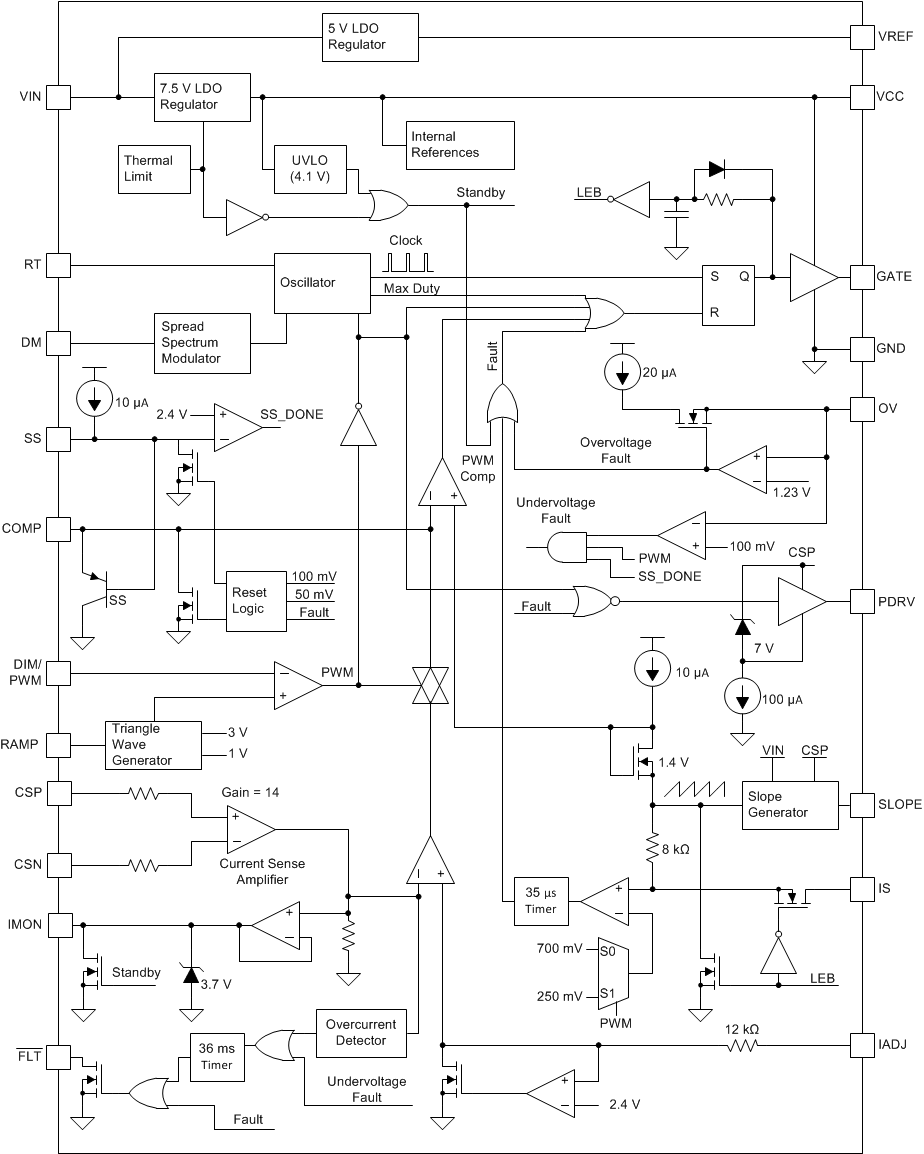
7.3 Feature Description
7.3.1 Internal Regulator and Undervoltage Lockout (UVLO)
The device incorporates a 65-V input voltage rated linear regulators to generate the 7.5 V (typ) VCC bias supply, the 5 V (typ) VREF reference supply and other internal reference voltages. The device monitors the VCC output to implement UVLO protection. Operation is enabled when VCC exceeds the 4.5-V (typ) threshold and is disabled when VCC drops below the 4.1-V (typ) threshold. The UVLO comparator provides 400 mV of hysteresis to avoid chatter during transitions. The UVLO thresholds are internally fixed and cannot be adjusted. An internal current limit circuit is implemented to protect the device during VCC pin short-circuit conditions. The VCC supply powers the internal circuitry and the N-channel gate driver output, GATE. Place a bypass capacitor in the range of 2.2 µF to 4.7 µF across the VCC output and GND to ensure proper operation. The regulator operates in dropout when input voltage VIN falls below 7.5 V forcing VCC to be lower than VIN by 300 mV for a 20-mA supply current. The VCC is a regulated output of the internal regulator and is not recommended to be driven from an external power supply.
The VREF supply is internally used to generate voltage thresholds for the RAMP generator circuit and to power some digital circuits. This supply can be used in conjunction with a resistor divider to set voltage levels for the IADJ pin and DIM/PWM pin to set LED current and PWM dimming duty cycle. It can also be used to bias external circuitry requiring a reference supply. The supply current is internally limited to protect the device from output overload and short-circuit conditions. Place a bypass capacitor in the range of 2.2 µF to 4.7 µF across the VREF output to GND to ensure proper operation.
The TPS92692 and TPS92692-Q1 devices incorporate features that simplify compliance with the CISPR and automotive EMI requirements. The devices have optional spread spectrum frequency modulation circuit that can be externally configured to reduce peak and average conducted and radiated EMI. The internal programmable oscillator has a range of 80 kHz to 800 kHz and can be tuned based on the EMI requirements. The devices are available in HTSSOP-20 package with an exposed pad to aid in thermal dissipation.
7.3.2 Oscillator
The switching frequency is programmable by a single external resistor connected between the RT pin and GND. To set a desired frequency, ƒSW (Hz), the resistor value can be calculated from Equation 1.

Figure 6 shows a graph of switching frequency versus resistance, RT. TI recommends a switching frequency setting between 80 kHz and 700 kHz for optimal performance over input and output voltage operating range and for best efficiency. Operation at higher switching frequencies requires careful selection of N-channel MOSFET characteristics as well as detailed analysis of switching losses.
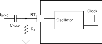 Figure 21. Oscillator Synchronization Through AC Coupling
The internal oscillator can be synchronized by AC coupling an external clock pulse to RT pin as shown in Figure 21. The positive going synchronization clock at the RT pin must exceed the RT sync threshold and the negative going synchronization clock at the RT pin must exceed the RT sync falling threshold to trip the internal synchronization pulse detector. TI recommends that the frequency of the external synchronization pulse is within ±20% of the internal oscillator frequency programmed by the RT resistor. TI recommends a minimum coupling capacitor of 100 nF and a typical pulse width of 100 ns for proper synchronization. In the case where external synchronization clock is lost the internal oscillator takes control of the switching rate based on the RT resistor to maintain output current regulation. The RT resistor is always required whether the oscillator is free running or externally synchronized.
7.3.3 Spread Spectrum Frequency Modulation
The TPS92692 and TPS92692-Q1 devices provide a frequency dithering option that is enabled by connecting a capacitor from the DM pin to GND. A triangle waveform centered at 1 V is generated across the CDM capacitor. The triangle waveform modulates the oscillator frequency by ± 15% of the nominal frequency set by an external timing resistor, RT. The CDM capacitance value sets the rate of the low frequency modulation. To achieve maximum attenuation in average EMI scan set modulation frequency ranging from 100 Hz to 1.2 kHz. The low modulating frequency has little impact on the quasi-peak EMI scan. Set the modulation frequency to 10 KHz or higher to achieve attenuation for quasi-peak EMI measurements. The modulation frequency higher than the receiver resolution bandwidth (RBW) of 9 kHz only impacts the quasi-peak EMI scan and has little impact on the average measurement. The device simplifies EMI compliance by providing the means to tune the modulation frequency based on measured EMI signature. Equation 2 calculates the CDM capacitance required to set the modulation frequency, fMOD (Hz).

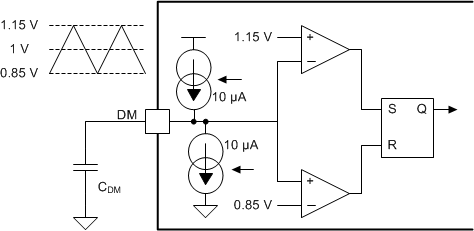 Figure 22. Frequency Dither Operation
Connect the DM pin to GND to disable frequency dither circuit operation. Internal frequency dithering is not supported when the devices are synchronized based on an external clock signal.
7.3.4 Gate Driver
The TPS92692 and TPS92692-Q1 devices contain a N-channel gate driver that switches the output VGATE between VCC and GND. A peak source and sink current of 500 mA allows controlled slew-rate of the MOSFET gate and drain node voltages, limiting the conducted and radiated EMI generated by switching.
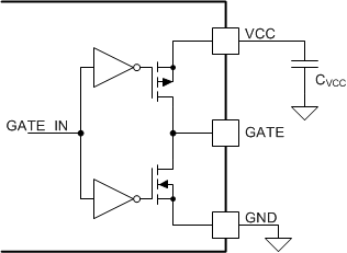 Figure 23. Push-Pull N-Channel Gate Driver Circuit
The gate driver supply current ICC(GATE) depends on the total gate drive charge (QG) of the MOSFET and the operating frequency of the converter, ƒSW,  . Choose a MOSFET with a low gate charge specification to limit the junction temperature rise and switch transition losses.
It is important to consider the MOSFET threshold voltage when operating in the dropout region when the input voltage, VIN, is below the VCC regulation level. TI recommends a logic level device with a threshold voltage below 5 V when the device is required to operate at an input voltage less than 7 V.
7.3.5 Rail-to-Rail Current Sense Amplifier
The internal rail-to-rail current sense amplifier measures the average LED current based on the differential voltage drop between the CSP and CSN inputs over a common mode range of 0 V to 65 V. The differential voltage, V(CSP-CSN), is amplified by a voltage-gain factor of 14 and is connected to the negative input of the transconductance error amplifier. Accurate LED current feedback is achieved by limiting the cumulative input offset voltage, (represented by the sum of the voltage-gain error, the intrinsic current sense offset voltage, and the transconductance error amplifier offset voltage) to less than 5 mV over the recommended common-mode voltage, and temperature range.
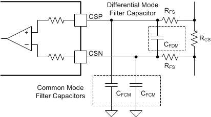 Figure 24. Current Sense Amplifier Input Filter Options
An optional common-mode or differential mode low-pass filter implementation, as shown in Figure 24, can be used to smooth out the effects of large output current ripple and switching current spikes caused by diode reverse recovery. TI recommends a filter resistance in the range of 10 Ω to 100 Ω to limit the additional offset caused by amplifier bias current mismatch to achieve the best accuracy and line regulation.
7.3.6 Transconductance Error Amplifier
The internal transconductance amplifier generates an error signal proportional to the difference between the LED current sense feedback voltage and the external IADJ input voltage. The output of the error amplifier is connected to an external compensation network to achieve closed-loop LED current regulation. In most LED driver applications a simple integral compensation circuit consisting of a capacitor connected from COMP output to GND provides a stable response over wide range of operating conditions. TI recommends a capacitor value between 10 nF and 100 nF as a good starting point. To achieve higher closed-loop bandwidth a proportional-integral compensator, consisting of a series resistor and a capacitor network connected across the COMP output and GND, is required. Based on the converter topology, tune the compensation network to achieve a minimum of 60° of phase margin and 10 dB of gain margin. The Application and Implementation section includes a summarized detailed design procedure.
7.3.7 Switch Current Sense
The IS input pin monitors the main MOSFET current to implement peak current mode control. The GATE output duty cycle is derived by comparing the peak switch current, measured by the RIS resistor, to the internal COMP voltage threshold. An internal slope signal, VSL, generated by slope compensation circuit is added to the measured sense voltage, VIS, to prevent subharmonic oscillations for duty cycles greater than 50%. An internal blanking circuit prevents MOSFET switching current spike propagation and premature termination of duty cycle by internally shunting the IS input for 150 ns after the beginning of the new switching period. For additional noise suppression connect an external low-pass RC filter with resistor values ranging from 100 Ω to 500 Ω and a 1000 pF capacitor. The external RC filter ensures proper operation when operating in the dropout region (VIN less than 7 V).
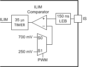 Figure 25. Switch Current Limit Circuit
Cycle-by-cycle current limit is accomplished by a redundant internal comparator. The current limit threshold is set based on the status of internal PWM signal. The current limit threshold is set to 250 mV (typ) when PWM signal is high and to 700 mV (typ) when PWM signal is low. The transition between the two thresholds work in conjunction with slope compensation and the error amplifier circuit to allow for higher inductor current immediately after the PWM transition and to improve LED current transient response during PWM dimming. Refer to the DIM/PWM Input section for details on PWM Dimming operation.
The device immediately terminates the GATE and PDRV output when the IS input voltage, VIS, exceeds the threshold value. Upon a current limit event, the SS and COMP pin are internally grounded to reset the state of the controller. The GATE output is enabled after the expiration of the 35-µs internal fault timer and a new start-up sequence is initiated through the SS pin. Equation 3 calculates the peak inductor current in the current limit.

7.3.8 Slope Compensation
Peak current mode based regulators are subject to sub-harmonic oscillations for duty cycle greater than 50%. To avoid this instability problem, the control scheme is modified by the addition of an artificial ramp to the sensed switch current waveform. The slope of the artificial ramp required is dependent on the input voltage, VIN, output voltage, VO, inductor, L, and switch current sense resistor, RIS. The devices incorporate an adaptive slope compensation technique that modifies the slope of the artificial ramp generated based on the input voltage, VIN and output voltage measured at CSP pin, VCSP, thus greatly simplifying the design for common LED driver topologies, such as boost, buck-boost, and boost-to-battery. The magnitude of the internal ramp signal can be calculated as follows:

where
- D is the converter duty cycle
The resistor, RSLOPE provides the flexibility to set the slope of the internal artificial ramp based on the inductance value, L and the LED driver topology. The Application and Implementation section includes detailed calculations for the resistor, RSLOPE, based on the LED driver topology. The SLOPE pin cannot be left floating.
7.3.9 Analog Adjust Input
The voltage across the LED current sense resistor, V(CSP–CSN), is regulated to the analog adjust input voltage, VIADJ, scaled by the current sense amplifier voltage gain of 14. The LED current can be linearly adjusted by varying the voltage on IADJ pin from 140 mV to 2.25 V using either a resistor divider from VREF or a voltage source. The IADJ pin can be connected to VREF through an external resistor to set LED current based on the 2.4-V internal reference voltage. This device offers different methods to set the IADJ voltage. Figure 27 shows how the IADJ input can be used in conjunction with a NTC resistor to implement thermal foldback protection. A PWM signal in conjunction with first- or second-order low-pass filter can be used to program the IADJ voltage as shown in Figure 28).
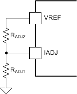 Figure 26. Static Reference Setting Resistor Divider From VCC
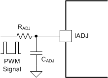 Figure 28. Analog Dimming Achieved By Low-pass Filtering External PWM Signal
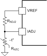 Figure 27. Thermal Fold-back Circuit Using External NTC Resistor
7.3.10 DIM/PWM Input
The TPS92692 and TPS92692-Q1 devices incorporate a PWM generator circuit to facilitate analog voltage to PWM duty cycle translation. The dimming frequency is set by connecting a capacitor from RAMP pin to GND. The dimming frequency, fDIM, can be calculated as follows:

The internal PWM signal can be varied from 0% to 100% by setting the DIM/PWM pin voltage between 1 V and 3 V. Equation 6 describes the relationship between DIM/PWM pin voltage, VDIM and internal PWM duty cycle, DPWM(INT).

For improved dimming accuracy, use the VREF pin and a resistor divider to set the DIM/PWM pin voltage, VDIM, and the corresponding duty cycle. The device can be configured to step the duty cycle between 100% and the programmed value by diode connecting the external control signal, VCTRL, to the DIM/PWM pin, as shown in Figure 29. The external control signal, of amplitude 3-V, is usually generated by the command module and is based on the light output required by the application.
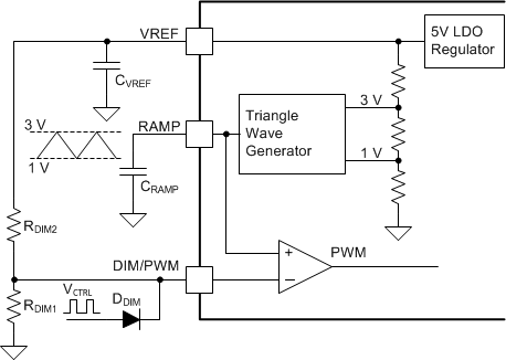 Figure 29. PWM Dimming Using Internal PWM Generator
The devices can be configured to be compatible with external PWM signal, VPWM(EXT), where the LED current is modulated based on the duty cycle, DPWM(EXT). To enable direct PWM, it is required to disable the internal triangle wave generator by connecting a 249-kΩ resistor from RAMP pin to GND. In this case, the internal comparator threshold is set to 2.49-V and the internal PWM duty cycle, DPWM(INT), is controlled by the external PWM command. The RAMP pin cannot be left floating.
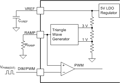 Figure 30. Direct PWM Dimming
The internal PWM signal, VPWM controls the GATE and PDRV outputs. Forcing VPWM in a logic low state turns off switching, parks the oscillator, disconnects the COMP pin, and sets the PDRV output to VCSP in order to maintain the charge on the compensation network and output capacitors. On the rising edge of the PWM voltage (VPWM set to logic level high), the GATE and PDRV outputs are enabled to ramp the inductor current to the previous steady-state value. The COMP pin is connected and the error amplifier and oscillator are enabled only when the switch current sense voltage VIS exceeds the COMP voltage, VCOMP, thus immediately forcing the converter into steady-state operation with minimum LED current overshoot. When dimming is not required, connect the DIM/PWM pin to the VCC pin. An internal pull-down resistor sets the input to logic-low and disables the device when the pin is disconnected or left floating.
7.3.11 Series P-Channel FET Dimming Gate Driver Output
The PDRV output is a function of the internal PWM signal and is capable of sinking and sourcing up to 50 mA of peak current to control a high-side series connected P-channel dimming FET. The PDRV switches between VCSP and (VCSP– 7 V) based on the status of PWM signal to completely turn-off and turn-on the external P-channel dimming FET. The series dimming FET is required to achieve high contrast ratio as it ensures fast rise and fall times of the LED current in response to the PWM input. Without any dimming FET, the rise and fall times are limited by the inductor slew rate and the closed-loop bandwidth of the system. Leave the PDRV pin unconnected if not used.
7.3.12 Soft-Start
The soft-start feature helps the regulator gradually reach the steady-state operating point, thus reducing startup stresses and surges. The devices clamp the COMP pin to the SS pin, separated by a diode, until LED current nears the regulation threshold. The internal 10-µA soft-start current source gradually increases the voltage on an external soft-start capacitor CSS connected to the SS pin. This results in a gradual rise of the COMP voltage from GND.
The internal 10-µA current source turns on when VCC exceeds the UVLO threshold. At the beginning of the soft-start sequence, the SS pull-down switch is active and is released when the voltage VSS drops below 50 mV. The SS pin can also be pulled down by an external switch to stop switching. When the SS pin is externally driven to enable switching, the slew-rate on the COMP pin is controlled by the compensation capacitor. In this case, the startup duration and LED current transient is controlled by tunning the compensation network. It is essential to ensure that the softstart duration is longer than the time required to charge the output capacitor when selecting the soft-start capacitor, CSS and the compensation capacitor, CCOMP.
7.3.13 Current Monitor Output
The IMON pin voltage represents the LED current measured by the rail-to-rail current sense amplifier across the external current shunt resistor. The linear relationship between the IMON voltage and LED current includes the amplifier gain-factor of 14 (see Feature Description section). The IMON output can be connected to an external microcontroller or comparator to facilitate LED open, short, or cable harness fault detection and mitigation. The IMON voltage is internally clamped to 3.7 V.
7.3.14 Output Overvoltage Protection
The TPS92692 and TPS92692-Q1 devices include a dedicated OV pin which can be used for either input or output overvoltage protection. This pin features a precision 1.228 V (typ) threshold with 20-µA (typ) of hysteresis current. The overvoltage threshold limit is set by a resistor divider network from the input or output terminal to GND. When the OV pin voltage exceeds the reference threshold, the GATE pin is immediately pulled low, the PDRV output is disabled, and the SS and COMP capacitors are discharged. The GATE and PDRV outputs are enabled and a new startup sequence is initiated after the voltage drops below the hysteresis threshold set by the 20-µA source current and the external resistor divider.
7.3.15 Output Short-circuit Protection
The device monitors the output of the current sense amplifier and the output voltage via OV pin to determine LED Short-circuit fault. The device signals an output overcurrent fault when the voltage across the current sense amplifier, (V(CSP-CSN)), exceeds the regulation set point based on the IADJ pin voltage, VIADJ. The overcurrent fault threshold is calculated as follows:

The device also indicates a short-circuit condition when the voltage across the OV pin and GND falls below 100 mV. In this case, the output voltage, VO, is below the undervoltage fault threshold determined based on the resistor divider connected to the OV pin.

The devices indicate a fault by forcing the open-drain fault indicator FLT pin to GND and initiating a 36-ms timer. The devices do not internally initiate any protection action and continue to operate until externally disabled by pulling SS pin to GND. This provides maximum design flexibility to enable user defined fault protection by using either the fault indicator output, FLT, or the analog IMON output based on the LED driver topology and end application.
The undervoltage fault detection circuit is internally disable based on the SS pin voltage and internal PWM status. The fault blanking circuit is designed to prevent false undervoltage detection during the startup sequence and PWM dimming operation.
7.3.16 Thermal Protection
Internal thermal shutdown circuitry is implemented to protect the controller in the event the maximum junction temperature is exceeded. When activated, typically at 175°C, the controller is forced into a shutdown mode, disabling the internal regulator. This feature is designed to prevent overheating and damage to the device.
7.3.17 Fault Indicator (FLT)
The devices include an open-drain output to indicate fault conditions. The FLT pin goes low under the following conditions:
- Overvoltage across the LED string (VOV> 1.24 V)
- Under voltage across the LED string (VOV< 100 mV)
- Overcurrent across the LED string (14 × V(CSP-CSN) > 1.5 × VIADJ)
- Cycle-by-cycle switch current limit condition (VIS > 250 mV)
The FLT pin goes high when the fault conditions ends or when the internal 36-ms timer expires. The status of the FLT under different fault conditions is summarized in the Device Functional Modes section.
7.4 Device Functional Modes
The following table summarizes the device behavior under fault condition.
Table 1. Fault Descriptions
| FAULT | DETECTION | ACTION |
|---|---|---|
| Input undervoltage (UVLO) | VCC(RISE) < 4.5 V | The device enters the standby state when the VCC voltage falls below the UVLO threshold. In standby state, GATE and PDRV outputs are disabled and the SS and COMP capacitors are discharged. FLT pin remains in high-impedance state. |
| VCC(FALL) < 4.1 V | ||
| Switch current limit | VIS > 250 mV | Cycle-by-cycle current limit is activated when the IS pin voltage exceeds 250 mV. The GATE and PDRV outputs are disabled, the SS and COMP pin capacitors are discharged and FLT pin is forced to ground. An internal 35-μs timer is activated. Soft-start sequence is initiated after expiration of the 35 μs timer period. |
| Thermal protection | TJ > 175°C | Internal thermal shutdown circuitry is activated when the junction temperature exceeds 175 °C. The controller is forced into a shutdown mode, disabling the internal regulators. A startup sequence is initiated when the junction temperature falls below 155˚C. The FLT pin remains in a high-impedance state. |
| Programmable output overvoltage protection | VOV > 1.228 V | When the OV pin voltage exceeds 1.228 V, GATE and PDRV outputs are disabled, SS and COMP capacitors are discharged, and the FLT pin is forced to GND. A soft-start sequence is initiated once the output voltage drops below the hysteresis threshold set by the 20 μA current source. |
| Fixed LED Overcurrent protection | V(CSP-CSN) > V((CSP-CSN),OCP) | The FLT pin is forced to ground for 36-ms when the LED current exceeds 1.5 times the regulation set point. The FLT pin is released after timer expires. Under sustained short-circuit condition, the FLT pin transitions between a high-impedance state and ground until the fault is cleared. Device continues to operate while in this condition. |
| Output undervoltage protection | VOV < 100 mV | The FLT pin is forced to ground for 36-ms when OV pin voltage drops below 100 mV. The FLT pin is released after timer expires. Under sustained short-circuit condition, the FLT pin transitions between the high-impedance state and ground until fault is cleared. Device continues to operate while in this condition. |
| Programmable LED overcurrent protection | VIMON > VIADJ | Current monitor output (IMON) can be used to externally program current limit. The IMON output can be connected to an external microcontroller or comparator to facilitate LED open, short, or cable harness fault detection. |
| COMP pin short to ground | VCOMP < 1.6 V | Switching is disabled when COMP voltage falls below 1.6 V. The FLT pin remains a in high-impedance state. |
| VREF pin short to ground | VREF < 2.0 V | The device enters standby when the VCC voltage falls below the UVLO threshold. In the standby state, GATE and PDRV outputs are disabled and the SS and COMP capacitors are discharged. The FLT pin will remain in a high-impedance state. |
7.4.1 Hiccup Mode Short-circuit Protection
Connecting the FLT pin to the SS pin enables hiccup mode operation under output short-circuit conditions.
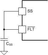 Figure 31. Hiccup Mode Short-Circuit Protection
On detection of output short-circuit fault, the FLT pin forces the SS pin to GND (VSS < 50 mV) and disables GATE and PDRV outputs for 36-ms. Upon timer expiration, the FLT pin is released and a new soft start sequence is initiated. Under sustained fault conditions the device operates in hiccup mode, attempting to recover after every 36-ms period.
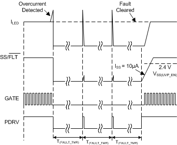 Figure 32. Output Overcurrent Fault Protection
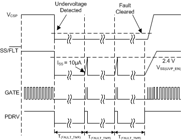 Figure 33. Output Undervoltage Fault Protection
7.4.2 Fault Indication Mode
The FLT pin output can be setup to indicate fault status to a microcontroller and aid in fault diagnostics and protection. In case of a fault, the FLT pin is forced low when biased through an external resistor connected either to reference voltage output, VREF, or an external bias supply. When connected to VREF, the FLT pin is driven low when the device enters standby mode during UVLO, thermal shutdown, or VREF short-circuit conditions. The Fault Indicator (FLT) section lists fault diagnostics and system level faults.
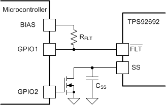 Figure 34. FLT Pin Interface With Microcontroller
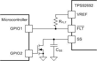 Figure 35. FLT Pin Interface With Microcontroller