ZHCSAM1F December   2012  – December 2017 TPS7A66-Q1 , TPS7A69-Q1

PRODUCTION DATA.  

  1. 特性
  2. 应用
  3. 说明
    1.     Device Images
      1.      硬件启用选项
      2.      输入电压感测选项
  4. 修订历史记录
  5. Pin Configuration and Functions
    1.     Pin Functions
  6. Specifications
    1. 6.1 Absolute Maximum Ratings
    2. 6.2 ESD Ratings
    3. 6.3 Recommended Operating Conditions
    4. 6.4 Thermal Information
    5. 6.5 Electrical Characteristics
    6. 6.6 Switching Characteristics
    7. 6.7 Typical Characteristics
  7. Detailed Description
    1. 7.1 Overview
    2. 7.2 Functional Block Diagrams
    3. 7.3 Feature Description
      1. 7.3.1 Enable (EN)
      2. 7.3.2 Regulated Output (VOUT)
      3. 7.3.3 Power-On Reset (PG)
      4. 7.3.4 Reset Delay Timer (CT)
      5. 7.3.5 Sense Comparator (SI and SO for TPS7A69-Q1)
      6. 7.3.6 Adjustable Output Voltage (FB for TPS7A6601-Q1)
      7. 7.3.7 Undervoltage Shutdown
      8. 7.3.8 Low-Voltage Tracking
      9. 7.3.9 Thermal Shutdown
    4. 7.4 Device Functional Modes
      1. 7.4.1 Regulation
      2. 7.4.2 Disabled
      3. 7.4.3 Operation With V(VinUVLO)< VIN < VIN(min)
  8. Application and Implementation
    1. 8.1 Application Information
    2. 8.2 Typical Applications
      1. 8.2.1 TPS7A66-Q1 Typical Application
        1. 8.2.1.1 Design Requirements
        2. 8.2.1.2 Detailed Design Procedure
          1. 8.2.1.2.1 Input Capacitor
          2. 8.2.1.2.2 Output Capacitor
        3. 8.2.1.3 Application Curve
      2. 8.2.2 TPS7A69-Q1 Typical Application
        1. 8.2.2.1 Design Requirements
        2. 8.2.2.2 Detailed Design Procedure
          1. 8.2.2.2.1 Low-Voltage Tracking Threshold
        3. 8.2.2.3 Application Curve
  9. Power Supply Recommendations
  10. 10Layout
    1. 10.1 Layout Guidelines
      1. 10.1.1 Package Mounting
      2. 10.1.2 Board Layout Recommendations to Improve PSRR and Noise Performance
    2. 10.2 Layout Examples
    3. 10.3 Power Dissipation and Thermal Considerations
  11. 11器件和文档支持
    1. 11.1 相关链接
    2. 11.2 接收文档更新通知
    3. 11.3 社区资源
    4. 11.4 商标
    5. 11.5 静电放电警告
    6. 11.6 Glossary
  12. 12机械、封装和可订购信息

封装选项

机械数据 (封装 | 引脚)
散热焊盘机械数据 (封装 | 引脚)
订购信息

Typical Characteristics

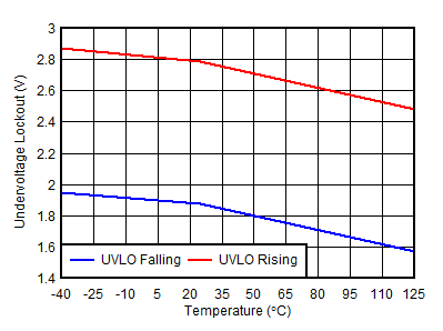
TPS7A66-Q1 TPS7A69-Q1 UVLO-01.gif
Figure 1. UVLO Thresholds vs Temperature
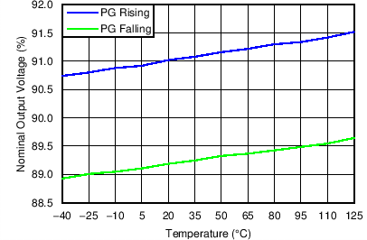
TPS7A66-Q1 TPS7A69-Q1 C001_SLVSBL0.png
Figure 3. Power-Good Threshold Voltage vs Temperature (VIN = 14 V, No Load)
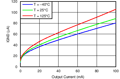
TPS7A66-Q1 TPS7A69-Q1 C003_SLVSBL0.png
Figure 5. Ground Current vs Output Current (VIN = 14 V)
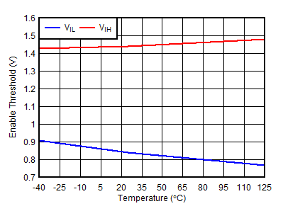
TPS7A66-Q1 TPS7A69-Q1 Ven Thresh-01.gif
Figure 2. Enable Thresholds vs Temperature
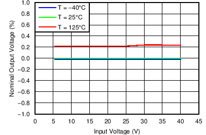
TPS7A66-Q1 TPS7A69-Q1 C002_SLVSBL0.png
Figure 4. Line Regulation (VIN = 14 V, IL = 1 mA)
TPS7A66-Q1 TPS7A69-Q1 C004_SLVSBL0.png
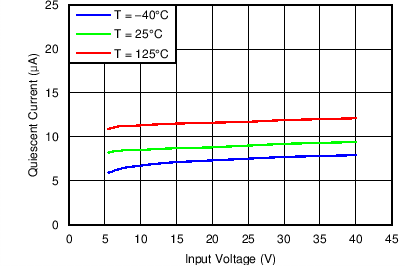
Figure 6. Quiescent Current vs Input Voltage (IL = 0)
TPS7A66-Q1 TPS7A69-Q1 C005_SLVSBL0.png
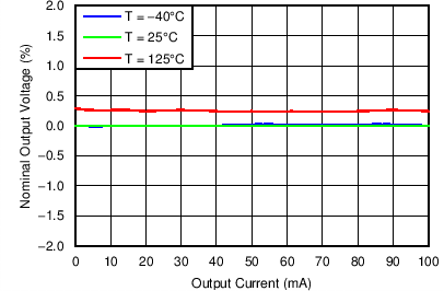
Figure 7. Load Regulation (VIN = 14 V)
TPS7A66-Q1 TPS7A69-Q1 C007_SLVSBL0.png
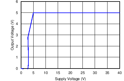
Figure 9. Output Voltage vs Supply Voltage
(Fixed 5-V Version, IL = 0)
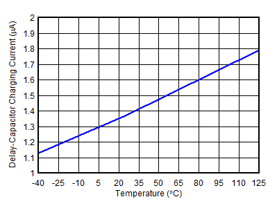
TPS7A66-Q1 TPS7A69-Q1 Ict-01.gif
Figure 11. CT Charging Current (VCT = 0)
TPS7A66-Q1 TPS7A69-Q1 C009_SLVSBL0.png
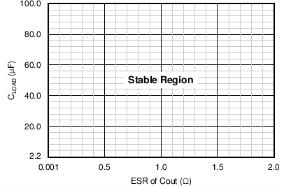
Figure 13. Load Capacitance vs ESR Stability
TPS7A66-Q1 TPS7A69-Q1 Scope-02_SLVSBL0.gif
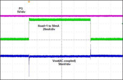
All oscilloscope waveforms were taken at room temperature.
Figure 15. Load Transient Response, 10 ms/div
TPS7A66-Q1 TPS7A69-Q1 Scope-04_SLVSBL0.gif
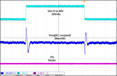
All oscilloscope waveforms were taken at room temperature.
Figure 17. Line Transient Response, IL = 1 mA, 1 V/µs
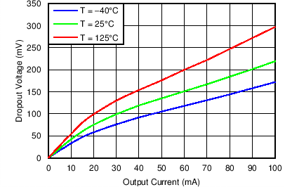
TPS7A66-Q1 TPS7A69-Q1 C006_SLVSBL0.png
Figure 8. Dropout Voltage vs Output Current (VIN = 4 V)
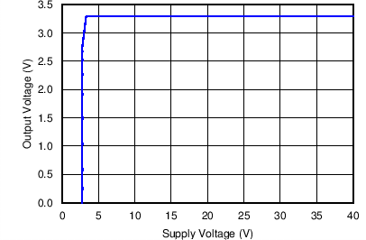
TPS7A66-Q1 TPS7A69-Q1 C008_SLVSBL0.png
Figure 10. Output Voltage vs Supply Voltage
(Fixed 3.3-V Version, IL = 0)
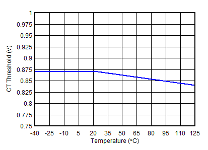
TPS7A66-Q1 TPS7A69-Q1 Vct-01.gif
Figure 12. CT Charging Threshold
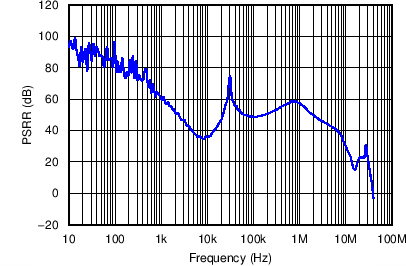
TPS7A66-Q1 TPS7A69-Q1 C010_SLVSBL0.png
Figure 14. Power-Supply Rejection Ratio vs Frequency
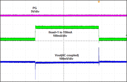
TPS7A66-Q1 TPS7A69-Q1 Scope-03_SLVSBL0.gif
All oscilloscope waveforms were taken at room temperature.
Figure 16. Load Transient Response, 10 ms/div
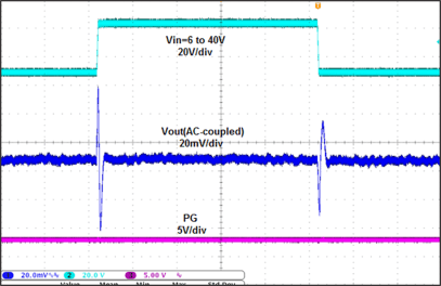
TPS7A66-Q1 TPS7A69-Q1 Scope-05_SLVSBL0.gif
All oscilloscope waveforms were taken at room temperature.
Figure 18. Line Transient Response, IL = 10 mA, 1 V/µs