ZHCS235D December 2011 – April 2015 TPS7A33
PRODUCTION DATA.
- 1 特性
- 2 应用
- 3 说明
- 4 修订历史记录
- 5 Pin Configuration and Functions
- 6 Specifications
- 7 Detailed Description
-
8 Application and Implementation
- 8.1
Application Information
- 8.1.1 Adjustable Operation
- 8.1.2 Capacitor Recommendations
- 8.1.3 Input and Output Capacitor Requirements
- 8.1.4 Noise Reduction and Feed-Forward Capacitor Requirements
- 8.1.5 Post DC-DC Converter Filtering
- 8.1.6 Audio Applications
- 8.1.7 Maximum AC Performance
- 8.1.8 Power-Supply Rejection
- 8.1.9 Output Noise
- 8.1.10 Transient Response
- 8.1.11 Power for Precision Analog
- 8.2 Typical Application
- 8.3 Do's and Don’ts
- 8.1
Application Information
- 9 Power Supply Recommendations
- 10Layout
- 11器件和文档支持
- 12机械封装和可订购信息
10 Layout
Layout is a critical part of good power-supply design. Several signal paths that conduct fast-changing currents or voltages can interact with stray inductance or parasitic capacitance to generate noise or degrade the power-supply performance. To help eliminate these problems, the IN pin should be bypassed to ground with a low ESR ceramic bypass capacitor with a X5R or X7R dielectric.
10.1 Layout Guidelines
10.1.1 Improve PSRR and Noise Performance
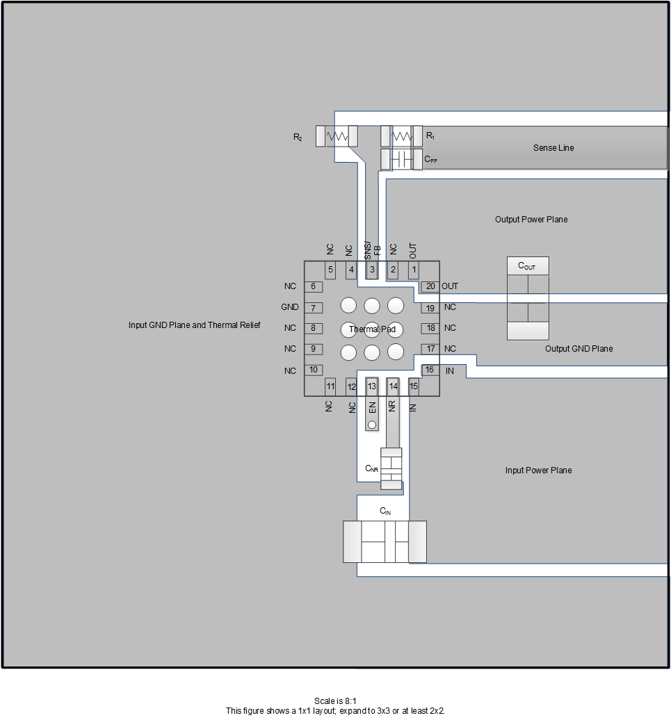
To improve AC performance such as PSRR, output noise, and transient response, TI recommends designing the board with separate planes for IN, OUT, and GND. The IN and OUT planes should be isolated from each other by a GND plane section. In addition, the ground connection for the output capacitor should connect directly to the GND pin of the device.
Equivalent series inductance (ESL) and equivalent series resistance (ESR) must be minimized in order to maximize performance and ensure stability. Every capacitor (CIN, COUT, CNR/SS, CFF) must be placed as close as possible to the device and on the same side of the PCB as the regulator itself.
Do not place any of the capacitors on the opposite side of the PCB from where the regulator is installed. The use of vias and long traces is strongly discouraged because they may impact system performance negatively and even cause instability.
10.2 Layout Example
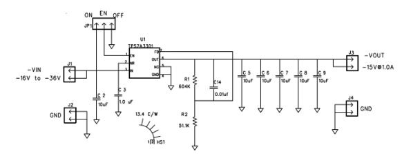
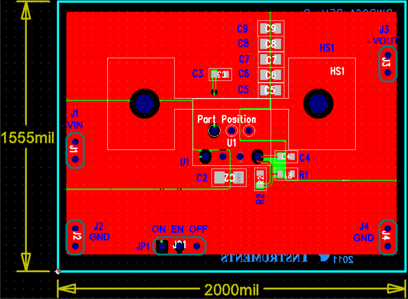
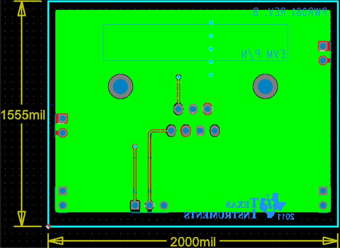
It may be possible to obtain acceptable performance with alternative PCB layouts; however, the layout shown in Figure 41 and the schematic shown in Figure 42 have been shown to produce good results and are meant as a guideline.
 Figure 40. TPS7A33 5-mm × 5-mm QFN-20 Layout Guideline
 Figure 43. Schematic for TPS7A33 TO-220 EVM PCB Layout Example
10.3 Thermal Performance and Heat Sink Selection
The primary TPS7A33 application is to provide ultralow-noise voltage rails to high-performance analog circuitry in order to maximize system accuracy and precision. The high-current and high-voltage characteristics of this regulator means that, often enough, high power (heat) is dissipated from the device itself. This heat, if dissipated into the PCB (as is the case with SMT packages), creates a temperature gradient in the surrounding area that causes nearby components to react to this temperature change (drift). In high-performance systems, such drift may degrade overall system accuracy and precision.
Compared to surface-mount packages, the TO-220 (KC) package allows for an external heat sink to be used to maximize thermal performance and keep heat from dissipating into the PCB.
The heat generated by the device is a result of the power dissipation, which depends on input voltage and load conditions. Power dissipation (PD) can be approximated by calculating the product of the output current times the voltage drop across the output pass element, as shown in Equation 4:

Heat flows from the device to the ambient air through many paths, each of which represents resistance to the heat flow; this effect is called thermal resistance.
The total thermal resistance of a system is defined by: θJA = (TJ – TA)/PD; where: θJA is the thermal resistance (in °C/W), TJ is the allowable juntion temperature of the device (in °C), TA is the maximum temperature of the ambient cooling air (in °C), and PD is the amount of power (heat) dissipated by the device (in W).
Whenever a heat sink is installed, the total thermal resistance (θJA) is the sum of all the individual resistances from the device, going through its case and heatsink to the ambient cooling air (θJA = θJC + θCS + θSA). Realistically, only two resistances can be controlled: θCS and θSA. Therefore, for a device with a known θJC, θCS and θSA become the main design variables in selecting a heat sink.
The thermal interface between the case and the heat sink (θCS) is controlled by selecting the correct heat-conducting material. Once the θCS is selected, the required thermal resistance from the heat sink to ambient is calculated by the following equation: θSA = [(TJ – TA)/PD] – [θJC+ θCS]. This information allows the most appropriate heat sink to be selected for any particular application.
10.4 Package Mounting
The TO-220 (KC) 7-lead, straight-formed package lead spacing poses a challenge when creating a suitable PCB footprint without bending the leads. Component forming pliers can be used to manually bend the package leads into a 7-lead stagger pattern with increased lead spacing that can be more easily used.
The TPS7A33 evaluation board layout can be used as a guideline on suitable PCB footprints, available at www.ti.com. Refer to the TPS7A3301EVM-061 user's guide for more information.

