ZHCSHU2B March 2018 – October 2018 TPS7A10
PRODUCTION DATA.
- 1 特性
- 2 应用
- 3 说明
- 4 修订历史记录
- 5 Pin Configuration and Functions
- 6 Specifications
- 7 Detailed Description
-
8 Application and Implementation
- 8.1 Application Information
- 8.2 Typical Application
- 9 Power Supply Recommendations
- 10Layout
- 11器件和文档支持
- 12机械、封装和可订购信息
封装选项
请参考 PDF 数据表获取器件具体的封装图。
机械数据 (封装 | 引脚)
- DSE|6
- YKA|5
散热焊盘机械数据 (封装 | 引脚)
订购信息
8.1.3 Load Transient Response
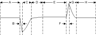
The load-step transient response is the output voltage response by the LDO to a step in load current while output voltage regulation is maintained. See Figure 9, Figure 10, Figure 11, and Figure 12 for typical load transient response. There are two key transitions during a load transient response: the transition from a light to a heavy load, and the transition from a heavy to a light load. The regions in Figure 39 are broken down as described in this section. Regions A, E, and H are where the output voltage is in steady-state operation.
 Figure 39. Load Transient Waveform
 During transitions from a light load to a heavy load:
- The initial voltage dip is a result of the depletion of the output capacitor charge and parasitic impedance to the output capacitor (region B)
- Recovery from the dip results from the LDO increasing the sourcing current, and leads to output voltage regulation (region C)
During transitions from a heavy load to a light load:
- The initial voltage rise results from the LDO sourcing a large current, and leads to the output capacitor charge to increase (region F)
- Recovery from the rise results from the LDO decreasing the sourcing current in combination with the load discharging the output capacitor (region G)
A larger output capacitance reduces the peaks during a load transient, but slows down the response time of the device. A larger dc load also reduces the peaks because the amplitude of the transition is lowered, and a higher current discharge path is provided for the output capacitor.