ZHCSJN7J October   2002  – May 2019 TPS795

PRODUCTION DATA.  

  1. 特性
  2. 应用
  3. 说明
    1.     Device Images
      1.      TPS79530 波纹抑制与频率
      2.      TPS79530 与频率
  4. 修订历史记录
  5. Pin Configuration and Functions
    1.     Pin Functions
  6. Specifications
    1. 6.1 Absolute Maximum Ratings
    2. 6.2 ESD Ratings
    3. 6.3 Recommended Operating Conditions
    4. 6.4 Thermal Information
    5. 6.5 Electrical Characteristics
    6. 6.6 Typical Characteristics
  7. Detailed Description
    1. 7.1 Overview
    2. 7.2 Functional Block Diagrams
    3. 7.3 Feature Description
      1. 7.3.1 Shutdown
      2. 7.3.2 Start-Up
      3. 7.3.3 Undervoltage Lockout (UVLO)
      4. 7.3.4 Regulator Protection
    4. 7.4 Device Functional Modes
      1. 7.4.1 Normal Operation
      2. 7.4.2 Dropout Operation
      3. 7.4.3 Disabled
  8. Application and Implementation
    1. 8.1 Application Information
    2. 8.2 Typical Application
      1. 8.2.1 Design Requirements
      2. 8.2.2 Detailed Design Procedure
        1. 8.2.2.1 Input and Output Capacitor Requirements
        2. 8.2.2.2 Output Noise
        3. 8.2.2.3 Dropout Voltage
        4. 8.2.2.4 Programming the TPS79501 Adjustable LDO Regulator
      3. 8.2.3 Application Curves
    3. 8.3 What to Do and What Not to Do
  9. Power Supply Recommendations
  10. 10Layout
    1. 10.1 Layout Guidelines
      1. 10.1.1 Board Layout Recommendation to Improve PSRR and Noise Performance
      2. 10.1.2 Regulator Mounting
      3. 10.1.3 Thermal Considerations
      4. 10.1.4 Estimating Junction Temperature
    2. 10.2 Layout Examples
  11. 11器件和文档支持
    1. 11.1 器件支持
      1. 11.1.1 开发支持
        1. 11.1.1.1 评估模块
        2. 11.1.1.2 Spice 模型
      2. 11.1.2 器件命名规则
    2. 11.2 文档支持
      1. 11.2.1 相关文档
    3. 11.3 接收文档更新通知
    4. 11.4 社区资源
    5. 11.5 商标
    6. 11.6 静电放电警告
    7. 11.7 Glossary
  12. 12机械、封装和可订购信息

封装选项

机械数据 (封装 | 引脚)
散热焊盘机械数据 (封装 | 引脚)
订购信息

Pin Configuration and Functions

DRB Package
8-Pin VSON
Top View
TPS795 po_3x3-son_lvs350.gif
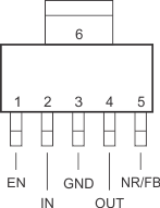
DCQ Package
6-Pin SOT-223
Top View
TPS795 po_sot223-5_lvs350.gif

Pin Functions

PIN I/O DESCRIPTION
NAME VSON SOT-223
IN 1, 2 2 I Unregulated input to the device
GND 6 3, 6 Regulator ground
EN 8 1 I Driving the enable pin (EN) high turns on the regulator. Driving this pin low puts the regulator into shutdown mode. EN can be connected to IN if not used.
NR 5 5 Noise-reduction pin for fixed versions only. Connecting an external capacitor to this pin bypasses noise generated by the internal bandgap, which improves power-supply rejection and reduces output noise. (Not available on adjustable versions.)
FB 5 5 I Feedback input voltage for the adjustable device.
(Not available on fixed voltage versions.)
OUT 3, 4 4 O Regulator output
N/C 7 No internal connection