SBVS038U September 2003 – January 2015 TPS736
PRODUCTION DATA.
- 1 Features
- 2 Applications
- 3 Description
- 4 Revision History
- 5 Pin Configuration and Functions
- 6 Specifications
- 7 Detailed Description
- 8 Application and Implementation
- 9 Power Supply Recommendations
- 10Layout
- 11Device and Documentation Support
- 12Mechanical, Packaging, and Orderable Information
封装选项
机械数据 (封装 | 引脚)
散热焊盘机械数据 (封装 | 引脚)
- DRB|8
订购信息
6 Specifications
6.1 Absolute Maximum Ratings
over operating junction temperature range (unless otherwise noted) (1)| MIN | MAX | UNIT | ||
|---|---|---|---|---|
| Voltage | VIN | –0.3 | +6.0 | V |
| VEN | –0.3 | +6.0 | V | |
| VOUT | –0.3 | +5.5 | V | |
| VNR, VFB | –0.3 | +6.0 | V | |
| Peak output current | IOUT | Internally limited | ||
| Output short-circuit duration | Indefinite | |||
| Continuous total power dissipation | PDISS | See Thermal Information | ||
| TJ | Junction temperature range | –55 | 150 | °C |
| Tstg | Storage temperature range | –65 | 150 | °C |
(1) Stresses beyond those listed under Absolute Maximum Ratings may cause permanent damage to the device. These are stress ratings only, which do not imply functional operation of the device at these or any other conditions beyond those indicated under Recommended Operating Conditions. Exposure to absolute-maximum-rated conditions for extended periods may affect device reliability. Electrical Characteristics Exposure to absolute maximum rated conditions for extended periods may affect device reliability
6.2 ESD Ratings
| VALUE | UNIT | |||
|---|---|---|---|---|
| V(ESD) | Electrostatic discharge | Human body model (HBM), per ANSI/ESDA/JEDEC JS-001, all pins(1) | ±2000 | V |
| Charged device model (CDM), per JEDEC specification JESD22-C101, all pins(2) | ±500 | |||
(1) JEDEC document JEP155 states that 500-V HBM allows safe manufacturing with a standard ESD control process.
(2) JEDEC document JEP157 states that 250-V CDM allows safe manufacturing with a standard ESD control process.
6.3 Recommended Operating Conditions
over operating junction temperature range (unless otherwise noted)| MIN | NOM | MAX | UNIT | ||
|---|---|---|---|---|---|
| VIN | Input supply voltage range | 1.7 | 5.5 | V | |
| IOUT | Output current | 0 | 500 | mA | |
| TJ | Operating junction temperature | –40 | 125 | °C | |
6.4 Thermal Information
| THERMAL METRIC(1)(2) | TPS736(3) | UNIT | |||
|---|---|---|---|---|---|
| DRB/SON | DCQ/SOT223 | DBV/SOT23 | |||
| 8 PINS | 6 PINS | 5 PINS | |||
| RθJA | Junction-to-ambient thermal resistance(4) | 52.8 | 118.7 | 221.9 | °C/W |
| RθJC(top) | Junction-to-case (top) thermal resistance(5) | 60.4 | 64.9 | 74.9 | |
| RθJB | Junction-to-board thermal resistance(6) | 28.4 | 65.0 | 51.9 | |
| ψJT | Junction-to-top characterization parameter(7) | 2.1 | 14.0 | 2.8 | |
| ψJB | Junction-to-board characterization parameter(8) | 28.6 | 63.8 | 51.1 | |
| RθJC(bot) | Junction-to-case (bottom) thermal resistance(9) | 12.0 | N/A | N/A | |
(1) For more information about traditional and new thermal metrics, see the IC Package Thermal Metrics application report, SPRA953.
(2) For thermal estimates of this device based on PCB copper area, see the TI PCB Thermal Calculator.
(3) Thermal data for the DRB, DCQ, and DRV packages are derived by thermal simulations based on JEDEC-standard methodology as specified in the JESD51 series. The following assumptions are used in the simulations:
-
i. DRB: The exposed pad is connected to the PCB ground layer through a 2x2 thermal via array.
ii. DCQ: The exposed pad is connected to the PCB ground layer through a 3x2 thermal via array.
iii. DBV: There is no exposed pad with the DBV package. -
i. DRB: The top and bottom copper layers are assumed to have a 20% thermal conductivity of copper representing a 20% copper coverage.
ii. DCQ: Each of top and bottom copper layers has a dedicated pattern for 20% copper coverage.
iii. DBV: The top and bottom copper layers are assumed to have a 20% thermal conductivity of copper representing a 20% copper coverage. - These data were generated with only a single device at the center of a JEDEC high-K (2s2p) board with 3in × 3in copper area. To understand the effects of the copper area on thermal performance, see the Power Dissipation section of this data sheet.
(4) The junction-to-ambient thermal resistance under natural convection is obtained in a simulation on a JEDEC-standard, high-K board, as specified in JESD51-7, in an environment described in JESD51-2a.
(5) The junction-to-case (top) thermal resistance is obtained by simulating a cold plate test on the top of the package. No specific JEDEC-standard test exists, but a close description can be found in the ANSI SEMI standard G30-88.
(6) The junction-to-board thermal resistance is obtained by simulating in an environment with a ring cold plate fixture to control the PCB temperature, as described in JESD51-8.
(7) The junction-to-top characterization parameter, ψJT, estimates the junction temperature of a device in a real system and is extracted from the simulation data to obtain θJA using a procedure described in JESD51-2a (sections 6 and 7).
(8) The junction-to-board characterization parameter, ψJB, estimates the junction temperature of a device in a real system and is extracted from the simulation data to obtain θJA using a procedure described in JESD51-2a (sections 6 and 7).
(9) The junction-to-case (bottom) thermal resistance is obtained by simulating a cold plate test on the exposed (power) pad. No specific JEDEC standard test exists, but a close description can be found in the ANSI SEMI standard G30-88.
6.5 Electrical Characteristics
Over operating temperature range (TJ = –40°C to 125°C), VIN = VOUT(nom) + 0.5 V(1), IOUT = 10 mA, VEN = 1.7 V, andCOUT = 0.1 μF, unless otherwise noted. Typical values are at TJ = 25°C.
| PARAMETER | TEST CONDITIONS | MIN | TYP | MAX | UNIT | |||
|---|---|---|---|---|---|---|---|---|
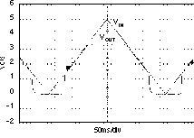
| VIN | Input voltage range(1)(2) | 1.7 | 5.5 | V | ||||
| VFB | Internal reference (TPS73601) | TJ = 25°C | 1.198 | 1.20 | 1.210 | V | ||
| VOUT | Output voltage range (TPS73601)(3) | VFB | 5.5 – VDO | V | ||||
| Accuracy(1)(4) | Nominal | TJ = 25°C | –0.5 | +0.5 | ||||
| over VIN, IOUT, and T |
VOUT + 0.5 V ≤ VIN ≤ 5.5 V; 10 mA ≤ IOUT ≤ 400 mA |
–1.0% | ±0.5% | +1.0% | ||||
| ΔVOUT(ΔVIN) | Line regulation(1) | VO(nom) + 0.5 V ≤ VIN ≤ 5.5 V | 0.01 | %/V | ||||
| ΔVOUT(ΔIOUT) | Load regulation | 1 mA ≤ IOUT ≤ 400 mA | 0.002 | %/mA | ||||
| 10 mA ≤ IOUT ≤ 400 mA | 0.0005 | |||||||
| VDO | Dropout voltage(5)
(VIN = VOUT(nom) – 0.1 V) |
IOUT = 400 mA | 75 | 200 | mV | |||
| ZO(do) | Output impedance in dropout | 1.7 V ≤ VIN ≤ VOUT + VDO | 0.25 | Ω | ||||
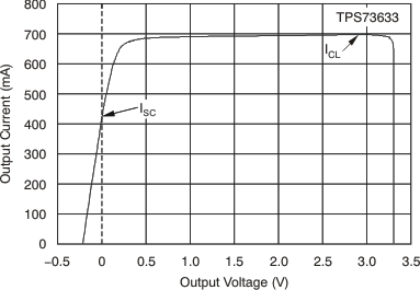
| ICL | Output current limit | VOUT = 0.9 × VOUT(nom) | 400 | 650 | 800 | mA | ||
| 3.6 V ≤ VIN ≤ 4.2 V, 0°C ≤ TJ ≤ 70°C | 500 | 800 | mA | |||||
| ISC | Short-circuit current | VOUT = 0 V | 450 | mA | ||||
| IREV | Reverse leakage current(6) (–IIN) | VEN ≤ 0.5 V, 0 V ≤ VIN ≤ VOUT | 0.1 | 10 | μA | |||
| IGND | GND pin current | IOUT = 10 mA (IQ) | 400 | 550 | μA | |||
| IOUT = 400 mA | 800 | 1000 | ||||||
| ISHDN | Shutdown current (IGND) | VEN ≤ 0.5 V, VOUT ≤ VIN ≤ 5.5, –40°C ≤ TJ ≤ 100°C |
0.02 | 1 | μA | |||
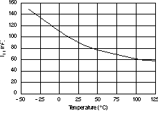
| IFB | FB pin current (TPS73601) | 0.1 | 0.3 | μA | ||||
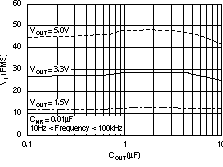
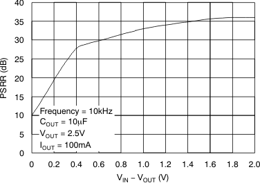
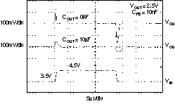
| PSRR | Power-supply rejection ratio (ripple rejection) | f = 100 Hz, IOUT = 400 mA | 58 | dB | ||||
| f = 10 kHz, IOUT = 400 mA | 37 | |||||||
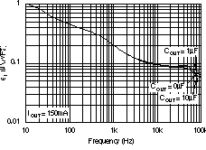
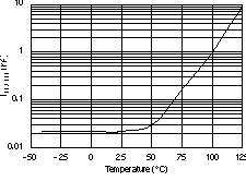
| Vn | Output noise voltage BW = 10Hz – 100KHz |
COUT = 10 μF, No CNR | 27 × VOUT | μVRMS | ||||
| COUT = 10 μF, CNR = 0.01 μF | 8.5 × VOUT | |||||||
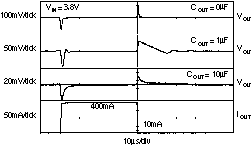
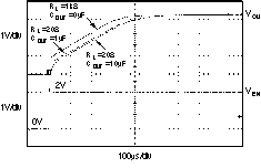
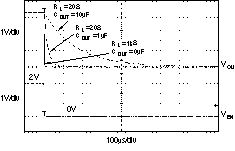
| tSTR | Startup time | VOUT = 3 V, RL = 30 Ω COUT = 1 μF, CNR = 0.01 μF | 600 | μs | ||||
| VEN(high) | EN pin high (enabled) | 1.7 | VIN | V | ||||
| VEN(low) | EN pin low (shutdown) | 0 | 0.5 | V | ||||
| IEN(high) | EN pin current (enabled) | VEN = 5.5 V | 0.02 | 0.1 | μA | |||
| TSD | Thermal shutdown temperature | Shutdown, temperature increasing | 160 | °C | ||||
| Reset, temperature decreasing | 140 | |||||||
| TJ | Operating junction temperature | –40 | 125 | °C | ||||
(1) Minimum VIN = VOUT + VDO or 1.7 V, whichever is greater.
(2) For VOUT(nom) < 1.6 V, when VIN ≤ 1.6 V, the output locks to VIN and may result in a damaging over-voltage level on the output. To avoid this situation, disable the device before powering down the VIN.
(3) TPS73601 is tested at VOUT = 2.5 V.
(4) Tolerance of external resistors not included in this specification.
(5) VDO is not measured for fixed output versions with VOUT(nom) < 1.8 V.
(6) Fixed-voltage versions only; refer to Application Information section for more information.
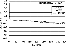
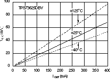
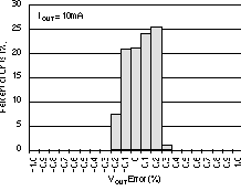
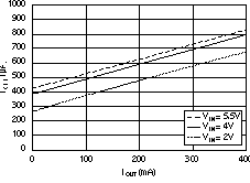
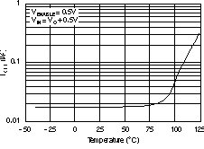
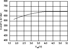
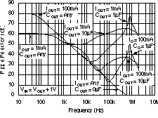
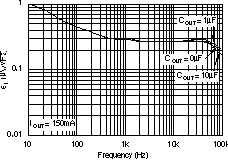
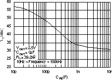
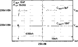
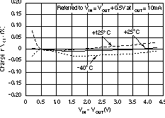
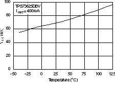
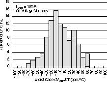
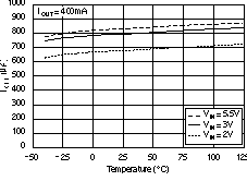
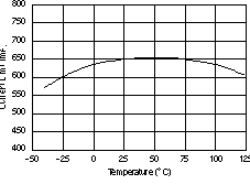
6.6 Typical Characteristics
For all voltage versions, at TJ = 25°C, VIN = VOUT(nom) + 0.5 V, IOUT = 10 mA, VEN = 1.7 V, and COUT = 0.1 μF, unless otherwise noted.