SBVS038U September 2003 – January 2015 TPS736
PRODUCTION DATA.
- 1 Features
- 2 Applications
- 3 Description
- 4 Revision History
- 5 Pin Configuration and Functions
- 6 Specifications
- 7 Detailed Description
- 8 Application and Implementation
- 9 Power Supply Recommendations
- 10Layout
- 11Device and Documentation Support
- 12Mechanical, Packaging, and Orderable Information
封装选项
机械数据 (封装 | 引脚)
散热焊盘机械数据 (封装 | 引脚)
- DRB|8
订购信息
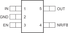
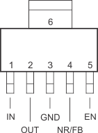
5 Pin Configuration and Functions
DBV Package
5-Pin SOT23
(Top View)
DCQ Package
6-Pin SOT223
(Top View)
DRB Package
8-Pin VSON
(Top View)
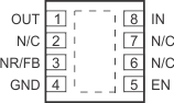
Pin Functions
| PIN | I/O | DESCRIPTION | |||
|---|---|---|---|---|---|
| NAME | NO. | ||||
| SOT23 | SOT223 | VSON | |||
| IN | 1 | 1 | 8 | I | Input supply |
| GND | 2 | 3, 6 | 4, Pad | — | Ground |
| EN | 3 | 5 | 5 | I | Driving the enable pin (EN) high turns on the regulator. Driving this pin low puts the regulator into shutdown mode. Refer to the Shutdown section for more details. EN can be connected to IN if not used. |
| NR | 4 | 4 | 3 | — | Fixed-voltage versions only. Connecting an external capacitor to this noise reduction pin bypasses noise generated by the internal bandgap, reducing output noise to very low levels. |
| FB | 4 | 4 | 3 | I | Adjustable-voltage version only. This pin is the input to the control loop error amplifier, and sets the output voltage of the device. |
| OUT | 5 | 2 | 1 | O | Output of the regulator. There are no output capacitor requirements for stability. |