SBVS038U September 2003 – January 2015 TPS736
PRODUCTION DATA.
- 1 Features
- 2 Applications
- 3 Description
- 4 Revision History
- 5 Pin Configuration and Functions
- 6 Specifications
- 7 Detailed Description
- 8 Application and Implementation
- 9 Power Supply Recommendations
- 10Layout
- 11Device and Documentation Support
- 12Mechanical, Packaging, and Orderable Information
封装选项
机械数据 (封装 | 引脚)
散热焊盘机械数据 (封装 | 引脚)
- DRB|8
订购信息
8 Application and Implementation
NOTE
Information in the following applications sections is not part of the TI component specification, and TI does not warrant its accuracy or completeness. TI’s customers are responsible for determining suitability of components for their purposes. Customers should validate and test their design implementation to confirm system functionality.
8.1 Application Information
The TPS736xx belongs to a family of new generation LDO regulators that use an NMOS pass transistor to achieve ultra-low-dropout performance, reverse current blockage, and freedom from output capacitor constraints. These features, combined with low noise and an enable input, make the TPS736xx ideal for portable applications. This regulator family offers a wide selection of fixed output voltage versions and an adjustable output version. All versions have thermal and over-current protection, including foldback current limit.
8.2 Typical Applications
Figure 31 shows the basic circuit connections for the fixed voltage models. Figure 32 gives the connections for the adjustable output version (TPS73601).
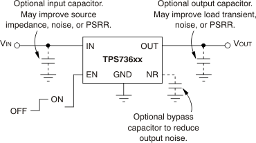 Figure 31. Typical Application Circuit for Fixed-Voltage Versions
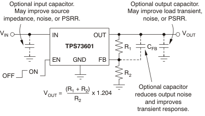 Figure 32. Typical Application Circuit for Adjustable-Voltage Version
8.2.1 Design Requirements
For this design example, use the parameters listed in Table 1 below as the input parameters.
Table 1. Design Parameters (Fixed-Voltage Version)
| PARAMETER | DESIGN REQUIREMENT |
|---|---|
| Input voltage | 5 V, ±3% |
| Output voltage | 3.3 V, ±1% |
| Output current | 500 mA (maximum), 20 mA (minimum) |
| RMS noise, 10 Hz to 100 kHz | < 30 μVRMS |
| Ambient temperature | 55°C (Maximum) |
Table 2. Design Parameters (Adjustable-Voltage Version)
| PARAMETER | DESIGN REQUIREMENT |
|---|---|
| Input voltage | 5 V, ±3%, provided by the dc/dc converter switching at 1 MHz |
| Output voltage | 2.5 V, ±1% |
| Output current | 0.4 A (maximum), 10 mA (minimum) |
| RMS noise, 10 Hz to 100 kHz | < 35 μVRMS |
| Ambient temperature | 55°C (Maximum) |
8.2.2 Detailed Design Procedure
The first step when designing with a linear regulator is to examine the maximum load current along with the input and output voltage requirements to determine if the device thermal and dropout voltage requirements can be met. At 0.5 A, the dropout voltage of the TPS73633 is a maximum of 200 mV over temperature; thus, the dropout headroom is sufficient for operation over both input and output voltage accuracy.
The maximum power dissipated in the linear regulator is the maximum voltage dropped across the pass element from the input to the output times the maximum load current. In this example, the maximum voltage drop across in the pass element is 5 V + 3% (5.15 V) minus 3.3 V – 1% (3.267 V) or 1.883 V. The power dissipated in the pass element is calculated by taking this voltage drop multiplied by the maximum load current. For this example, the maximum power dissipated in the linear regulator is 942 mW. Once the power dissipated in the linear regulator is known, the corresponding junction temperature rise can be calculated. To calculate the junction temperature rise above ambient, the power dissipated must be multiplied by the junction-to-ambient thermal resistance. For thermal resistance information please refer to Thermal Protection. For this example, using the DRB package, the maximum junction temperature rise is calculated to be 45°C. The maximum junction temperature rise is calculated by adding junction temperature rise to the maximum ambient temperature. In this example, the maximum junction temperature is 100°C. Keep in mind the maximum junction temperate must be below 125°C for reliable operation. Addition ground planes, added thermal vias, and air flow all help to lower the maximum junction temperature. Using the DCQ or DBV packages are not recommended for this application due to the excessive junction temperature rise that would be incurred.
To get the noise level below 30 µVRMS, a noise reduction capacitance (CNR) of 10 nF is selected along with an output capacitance of 10 μF. Referencing the Output Noise section, the RMS noise can be calculated to be 28 µVRMS.
Use of an input capacitor is optional. However, in systems where the input supply is located several inches away from the LDO, a small 0.1-µF input capacitor is recommended to negate the adverse effects that input supply inductance has on stability and ac performance.
In the same way as with designing with a fixed output voltage, the first step is to examine the maximum load current along with the input and output voltage requirements to determine if the device thermal and dropout voltage requirements are met. At 0.4 A, the maximum dropout voltage can be approximated by assuming a linear characteristic of the dropout voltage with load current. The maximum dropout voltage can be estimated to be 200 mV times the ratio of the load current to specified dropout voltage load current. For this example, the dropout can be estimated to be 200 mV × 400 mA/500 mA or 160 mV. Since the input voltage is 5 V and the output voltage is 2.5 V, there is more than sufficient voltage headroom to avoid dropout and maintain good PSRR.
The maximum power dissipated in the linear regulator is the maximum voltage dropped across the pass element from the input to the output times the maximum load current. In this example, the maximum voltage drop across in the pass element is 5 V + 3% (5.15 V) minus 2.5 V – 1% (2.475 V) or 2.675 V. The power dissipated in the pass element is calculated by taking this voltage drop multiplied by the maximum load current. For this example, the maximum power dissipated in the linear regulator is 1.07 W. Once the power dissipated in the linear regulator is known, the corresponding junction temperature rise can be calculated. To calculate the junction temperature rise above ambient, the power dissipated must be multiplied by the junction-to-ambient thermal resistance. For thermal resistance information, refer to Thermal Information. For this example, using the DRB package, the maximum junction temperature rise is calculated to be 51°C. The maximum junction temperature rise is calculated by adding junction temperature rise to the maximum ambient temperature. In this example, the maximum junction temperature is 106°C. Keep in mind the maximum junction temperate must be below 125°C for reliable operation. Addition ground planes, added thermal vias, and air flow all help to lower the maximum junction temperature. Using the DCQ or DBV packages are not recommended for this application due to the excessive junction temperature rise that would be incurred.
R1 and R2 can be calculated for any output voltage using the formula shown in Figure 32. Sample resistor values for common output voltages are shown in Figure 30.
For best accuracy, make the parallel combination of R1 and R2 approximately equal to 19 kΩ. This 19 kΩ, in addition to the internal 8-kΩ resistor, presents the same impedance to the error amp as the 27-kΩ bandgap reference output. This impedance helps compensate for leakages into the error amp terminals.
Using the values shown in Figure 40xx for a 2.5-V output results in a values of 39.2 kΩ for R1 and 36.5 kΩ for R2.
To get the noise level below 35 µVRMS, a noise reduction capacitance (CFF) of 10 nF is selected. Figure 25 should be used as a reference when selecting optimal value for CFF.
A 10-µF, low equivalent series resistance (ESR) ceramic X5R capacitor was used on the output of this design to minimize the output voltage droop during a low transient. Use of an input capacitor is optional. However, in systems where the input supply is located several inches away from the LDO, a small 0.1-µF input capacitor is recommended to negate the adverse effects that input supply inductance has on stability and ac performance. Refer to Input and Output Capacitor Requirements for additional information about input and output capacitor selection.
8.2.2.1 Input and Output Capacitor Requirements
Although an input capacitor is not required for stability, it is good analog design practice to connect a 0.1-μF to
1-μF, low ESR capacitor across the input supply near the regulator. This capacitor counteracts reactive input sources and improves transient response, noise rejection, and ripple rejection. A higher-value capacitor may be necessary if large, fast rise-time load transients are anticipated or the device is located several inches from the power source.
The TPS736xx does not require an output capacitor for stability and has maximum phase margin with no capacitor. It is designed to be stable for all available types and values of capacitors. In applications where multiple low ESR capacitors are in parallel, ringing may occur when the product of COUT and total ESR drops below 50 nΩF. Total ESR includes all parasitic resistances, including capacitor ESR and board, socket, and solder joint resistance. In most applications, the sum of capacitor ESR and trace resistance meets this requirement.
8.2.2.2 Dropout Voltage
The TPS736xx uses an NMOS pass transistor to achieve extremely low dropout. When (VIN – VOUT) is less than the dropout voltage (VDO), the NMOS pass device is in its linear region of operation and the input-to-output resistance is the RDS(on) of the NMOS pass element.
For large step changes in load current, the TPS736xx requires a larger voltage drop from VIN to VOUT to avoid degraded transient response. The boundary of this transient dropout region is approximately twice the dc dropout. Values of VIN – VOUT above this line ensure normal transient response.
Operating in the transient dropout region can cause an increase in recovery time. The time required to recover from a load transient is a function of the magnitude of the change in load current rate, the rate of change in load current, and the available headroom (VIN to VOUT voltage drop). Under worst-case conditions [full-scale instantaneous load change with (VIN – VOUT) close to dc dropout levels], the TPS736xx can take a couple of hundred microseconds to return to the specified regulation accuracy.
8.2.2.3 Transient Response
The low open-loop output impedance provided by the NMOS pass element in a voltage follower configuration allows operation without an output capacitor for many applications. As with any regulator, the addition of a capacitor (nominal value 1 μF) from the OUT pin to ground reduces undershoot magnitude but increase its duration. In the adjustable version, the addition of a capacitor, CFB, from the OUT pin to the FB pin also improves the transient response.
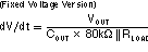
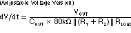
The TPS736xx does not have active pull-down when the output is over-voltage. This feature allows applications that connect higher voltage sources, such as alternate power supplies, to the output. This feature also results in an output overshoot of several percent if load current quickly drops to zero when a capacitor is connected to the output. The duration of overshoot can be reduced by adding a load resistor. The overshoot decays at a rate determined by output capacitor COUT and the internal/external load resistance. The rate of decay is given by:
8.2.3 Application Curves
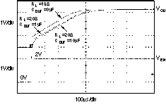 Figure 33. TPS73633 Turn-On Response
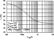
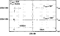
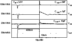 Figure 34. TPS73633 Load Transient Response