ZHCSI09S June 2010 – August 2018 TPS65911
PRODUCTION DATA.
- 1器件概述
- 2修订历史记录
- 3Device Comparison Table
- 4Pin Configuration and Functions
-
5Specifications
- 5.1 Absolute Maximum Ratings
- 5.2 ESD Ratings
- 5.3 Recommended Operating Conditions
- 5.4 Thermal Information
- 5.5 Electrical Characteristics: I/O Pullup and Pulldown
- 5.6 Electrical Characteristics: Digital I/O Voltage
- 5.7 Electrical Characteristics: Power Consumption
- 5.8 Electrical Characteristics: Power References and Thresholds
- 5.9 Electrical Characteristics: Thermal Monitoring and Shutdown
- 5.10 Electrical Characteristics: 32-kHz RTC Clock
- 5.11 Electrical Characteristics: Backup Battery Charger
- 5.12 Electrical Characteristics: VRTC LDO
- 5.13 Electrical Characteristics: VIO SMPS
- 5.14 Electrical Characteristics: VDD1 SMPS
- 5.15 Electrical Characteristics: VDD2 SMPS
- 5.16 Electrical Characteristics: VDDCtrl SMPS
- 5.17 Electrical Characteristics: LDO1 and LDO2
- 5.18 Electrical Characteristics: LDO3 and LDO4
- 5.19 Electrical Characteristics: LDO5
- 5.20 Electrical Characteristics: LDO6, LDO7, and LDO8
- 5.21 Timing and Switching Characteristics
-
6Detailed Description
- 6.1 Overview
- 6.2 Functional Block Diagram
- 6.3 Power Reference
- 6.4 Power Resources
- 6.5 Embedded Power Controller (EPC)
- 6.6 PWM and LED Generators
- 6.7 Dynamic Voltage Frequency Scaling and Adaptive Voltage Scaling Operation
- 6.8 32-kHz RTC Clock
- 6.9 Real Time Clock (RTC)
- 6.10 Backup Battery Management
- 6.11 Backup Registers
- 6.12 I2C Interface
- 6.13 Thermal Monitoring and Shutdown
- 6.14 Interrupts
- 6.15 Register Maps
-
7Applications, Implementation, and Layout
- 7.1 Application Information
- 7.2 Typical Application
- 7.3 Power Supply Recommendations
- 8器件和文档支持
- 9机械、封装和可订购信息
5.21.2 Switch-ON and Switch-OFF Sequences and Timing
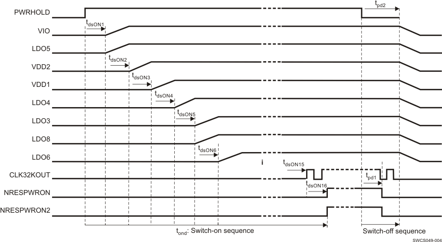
This section describes an example boot sequence. Each TPS65911x device supports a dedicated EEPROM boot sequence to match specific processor requirements. Fixed boot mode is the same in all TPS65911x devices. Boot mode selection is described in Section 6.5.2.

NOTE:
Figure 5-1 is for illustrative purposes only and does not describe any actual TPS65911x part number.Table 5-3 Switching Characteristics for Boot Sequence Example
| PARAMETER | TEST CONDITIONS | MIN | TYP | MAX | UNIT | |
|---|---|---|---|---|---|---|
| tdsON1 | PWRHOLD rising edge to VIO | LDO5 enable delay | 66 × tCK32k = 2060 | µs | ||
| tdsON2 | VIO to VDD2 enable delay | 64 × tCK32k = 2000 | µs | |||
| tdsON3 | VDD2 to VDD1 enable delay | 64 × tCK32k = 2000 | µs | |||
| tdsON4 | VDD1 to LDO4 enable delay | 64 × tCK32k = 2000 | µs | |||
| tdsON5 | LDO4 to LDO3, LDO8 enable delay | 64 × tCK32k = 2000 | µs | |||
| tdsON6 | LDO3 to LDO6 enable delay | 64 × tCK32k = 2000 | µs | |||
| tdsON7 | LDO6 to CLK32KOUT rising-edge delay | 9 × 64 × tCK32k = 18000 | µs | |||
| tdsON16 | CLK32KOUT to NRESPWON | NRESPWON2 rising-edge delay | 64 × tCK32k = 2000 | µs | ||
| tdsONT | Total switch-on delay | 32 | ms | |||
| tpd1 | PWRHOLD falling edge to NRESPWON | NRESPWON2 falling-edge delay | 2 × tCK32k = 62.5 | µs | ||
| tpd1b | NRESPWON falling edge to CLK32KOUT low delay | 3 × tCK32k = 92 | µs | |||
| tpd2 | PWRHOLD falling edge to supplies and reference disable delay | 5 × tCK32k = 154 | µs | |||