SLVSE55 November 2017 TPS65321A-Q1
PRODUCTION DATA.
- 1 Features
- 2 Applications
- 3 Description
- 4 Revision History
- 5 Pin Configuration and Functions
- 6 Specifications
-
7 Detailed Description
- 7.1 Overview
- 7.2 Functional Block Diagram
- 7.3
Feature Description
- 7.3.1
Buck Regulator
- 7.3.1.1 Fixed-Frequency PWM Control
- 7.3.1.2 Slope Compensation Output
- 7.3.1.3 Pulse-Skip Eco-mode™ Control Scheme
- 7.3.1.4 Dropout Mode Operation and Bootstrap Voltage (BOOT)
- 7.3.1.5 Error Amplifier
- 7.3.1.6 Voltage Reference
- 7.3.1.7 Adjusting the Output Voltage
- 7.3.1.8 Soft-Start Pin (SS)
- 7.3.1.9 Reset Output, nRST
- 7.3.1.10 Overload-Recovery Circuit
- 7.3.1.11 Constant Switching Frequency and Timing Resistor (RT/CLK Pin)
- 7.3.1.12 Overcurrent Protection and Frequency Shift
- 7.3.1.13 Selecting the Switching Frequency
- 7.3.1.14 How to Interface to RT/CLK Pin
- 7.3.1.15 Overvoltage Transient Protection
- 7.3.1.16 Small-Signal Model for Loop Response
- 7.3.1.17 Simple Small-Signal Model for Peak-Current Mode Control
- 7.3.1.18 Small-Signal Model for Frequency Compensation
- 7.3.2 LDO Regulator
- 7.3.3 Thermal Shutdown
- 7.3.4 Enable and Undervoltage Lockout
- 7.3.1
Buck Regulator
- 7.4 Device Functional Modes
-
8 Application and Implementation
- 8.1 Application Information
- 8.2
Typical Application
- 8.2.1
2-MHzSwitching Frequency, 9-V to 16-V Input, 3.3-V Output Buck Regulator, 5-V Output LDO Regulator
- 8.2.1.1 Design Requirements
- 8.2.1.2
Detailed Design Procedure
- 8.2.1.2.1 Switching Frequency Selection for the Buck Regulator
- 8.2.1.2.2 Output Inductor Selection for the Buck Regulator
- 8.2.1.2.3 Output Capacitor Selection for the Buck Regulator
- 8.2.1.2.4 Catch Diode Selection for the Buck Regulator
- 8.2.1.2.5 Input Capacitor Selection for the Buck Regulator
- 8.2.1.2.6 Soft-Start Capacitor Selection for the Buck Regulator
- 8.2.1.2.7 Bootstrap Capacitor Selection for the Buck Regulator
- 8.2.1.2.8 Output Voltage and Feedback Resistor Selection for the Buck Regulator
- 8.2.1.2.9 Frequency Compensation Selection for the Buck Regulator
- 8.2.1.2.10 LDO Regulator
- 8.2.1.2.11 Power Dissipation
- 8.2.1.2.12 Power Dissipation Losses of the LDO Regulator
- 8.2.1.2.13 Total Device Power Dissipation Losses and Junction Temperature
- 8.2.1.3 Application Curves
- 8.2.2 Design Example With 500-kHz Switching Frequency
- 8.2.1
2-MHzSwitching Frequency, 9-V to 16-V Input, 3.3-V Output Buck Regulator, 5-V Output LDO Regulator
- 9 Power Supply Recommendations
- 10Layout
- 11Device and Documentation Support
- 12Mechanical, Packaging, and Orderable Information
封装选项
请参考 PDF 数据表获取器件具体的封装图。
机械数据 (封装 | 引脚)
- PWP|14
散热焊盘机械数据 (封装 | 引脚)
- PWP|14
订购信息
10 Layout
10.1 Layout Guidelines
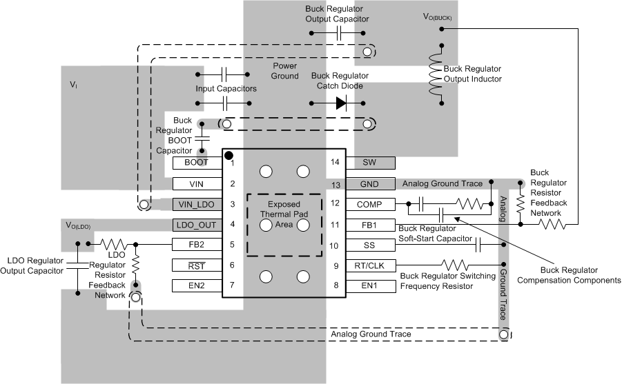
TI recommends the guidelines that follow for PCB layout of the TPS65321A-Q1 device.
- Inductor
- Input Filter Capacitors
- Feedback
- Traces and Ground Plane
Use a low-EMI inductor with a ferrite-type shielded core. Other types of inductors can also be used, however, these inductors must have low-EMI characteristics and be located away from the low-power traces and components in the circuit.
Locate input ceramic filter capacitors close to the VIN pin. TI recommends surface-mount capacitors to minimize lead length and reduce noise coupling.
Route the feedback trace for minimum interaction with any noise sources associated with the switching components. TI recommends to place the inductor away from the feedback trace to prevent creating an EMI noise source.
All power (high-current) traces must be as thick and short as possible. The inductor and output capacitors must be as close to each other as possible to reduce EMI radiated by the power traces because of high switching currents. In a two-sided PCB, TI recommends using ground planes on both sides of the PCB to help reduce noise and ground loop errors. The ground connection for the input capacitors, output capacitors, and device ground should connect to this ground plane, where the connection between input capacitors and the catch-diode is the most critical. In a multi-layer PCB, the ground plane separates the power plane (where high switching currents and components are) from the signal plane (where the feedback trace and components are) for improved performance. Also, arrange the components such that the switching-current loops curl in the same direction. Place the high-current components such that during conduction the current path is in the same direction. This placement prevents magnetic field reversal caused by the traces between the two half-cycles, and helps reduce radiated EMI.
10.2 Layout Example
 Figure 25. TPS65321A-Q1 Layout Example
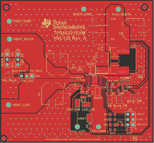
 Figure 26. TPS65321A-Q1 Layout Example
Top Side
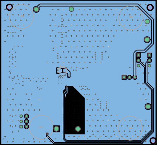
 Figure 27. TPS65321A-Q1 Layout Example
Bottom Side