SLVSE55 November 2017 TPS65321A-Q1
PRODUCTION DATA.
- 1 Features
- 2 Applications
- 3 Description
- 4 Revision History
- 5 Pin Configuration and Functions
- 6 Specifications
-
7 Detailed Description
- 7.1 Overview
- 7.2 Functional Block Diagram
- 7.3
Feature Description
- 7.3.1
Buck Regulator
- 7.3.1.1 Fixed-Frequency PWM Control
- 7.3.1.2 Slope Compensation Output
- 7.3.1.3 Pulse-Skip Eco-mode™ Control Scheme
- 7.3.1.4 Dropout Mode Operation and Bootstrap Voltage (BOOT)
- 7.3.1.5 Error Amplifier
- 7.3.1.6 Voltage Reference
- 7.3.1.7 Adjusting the Output Voltage
- 7.3.1.8 Soft-Start Pin (SS)
- 7.3.1.9 Reset Output, nRST
- 7.3.1.10 Overload-Recovery Circuit
- 7.3.1.11 Constant Switching Frequency and Timing Resistor (RT/CLK Pin)
- 7.3.1.12 Overcurrent Protection and Frequency Shift
- 7.3.1.13 Selecting the Switching Frequency
- 7.3.1.14 How to Interface to RT/CLK Pin
- 7.3.1.15 Overvoltage Transient Protection
- 7.3.1.16 Small-Signal Model for Loop Response
- 7.3.1.17 Simple Small-Signal Model for Peak-Current Mode Control
- 7.3.1.18 Small-Signal Model for Frequency Compensation
- 7.3.2 LDO Regulator
- 7.3.3 Thermal Shutdown
- 7.3.4 Enable and Undervoltage Lockout
- 7.3.1
Buck Regulator
- 7.4 Device Functional Modes
-
8 Application and Implementation
- 8.1 Application Information
- 8.2
Typical Application
- 8.2.1
2-MHzSwitching Frequency, 9-V to 16-V Input, 3.3-V Output Buck Regulator, 5-V Output LDO Regulator
- 8.2.1.1 Design Requirements
- 8.2.1.2
Detailed Design Procedure
- 8.2.1.2.1 Switching Frequency Selection for the Buck Regulator
- 8.2.1.2.2 Output Inductor Selection for the Buck Regulator
- 8.2.1.2.3 Output Capacitor Selection for the Buck Regulator
- 8.2.1.2.4 Catch Diode Selection for the Buck Regulator
- 8.2.1.2.5 Input Capacitor Selection for the Buck Regulator
- 8.2.1.2.6 Soft-Start Capacitor Selection for the Buck Regulator
- 8.2.1.2.7 Bootstrap Capacitor Selection for the Buck Regulator
- 8.2.1.2.8 Output Voltage and Feedback Resistor Selection for the Buck Regulator
- 8.2.1.2.9 Frequency Compensation Selection for the Buck Regulator
- 8.2.1.2.10 LDO Regulator
- 8.2.1.2.11 Power Dissipation
- 8.2.1.2.12 Power Dissipation Losses of the LDO Regulator
- 8.2.1.2.13 Total Device Power Dissipation Losses and Junction Temperature
- 8.2.1.3 Application Curves
- 8.2.2 Design Example With 500-kHz Switching Frequency
- 8.2.1
2-MHzSwitching Frequency, 9-V to 16-V Input, 3.3-V Output Buck Regulator, 5-V Output LDO Regulator
- 9 Power Supply Recommendations
- 10Layout
- 11Device and Documentation Support
- 12Mechanical, Packaging, and Orderable Information
封装选项
请参考 PDF 数据表获取器件具体的封装图。
机械数据 (封装 | 引脚)
- PWP|14
散热焊盘机械数据 (封装 | 引脚)
- PWP|14
订购信息
1 Features
- Qualified for Automotive Applications
- AEC-Q100 Qualified with the Following Results:
- Device Temperature Grade 1: –40°C to +125°C Ambient Operating Temperature
- Device HBM ESD Classification Level 2
- Device CDM ESD Classification Level C4B
- One High-VIN Step-Down DC-DC Converter
- Input Range of 3.6 V to 36 V
- 250-mΩ High-Side MOSFET
- Maximum Load Current 3.2 A, Output Adjustable 1.1 V to 20 V
- Adjustable Switching Frequency 100 kHz to 2.5 MHz
- Synchronizes to External Clock
- High Efficiency at Light Loads With Pulse-Skipping Eco-mode™ Control Scheme
- Maximum 140-µA Operating Quiescent Current
- Reset Output-Pin (Active Low, Open-Drain)
- One High-VIN Low-Dropout (LDO) Voltage Regulator
- Input Range of 3 V to 36 V
- 280-mA Current Capability With Typical 35-µA Quiescent Current in No-Load Condition
- Low-Dropout Voltage of 300 mV at
IO = 200 mA (Typical)
- Overcurrent Protection for Both Regulators
- Overtemperature Protection
- 14-Pin HTSSOP Package With PowerPAD™ Integrated Circuit Package
2 Applications
- Automotive Infotainment and Cluster
- Advanced Driver Assistance System (ADAS)
- Automotive Telematics, eCall
3 Description
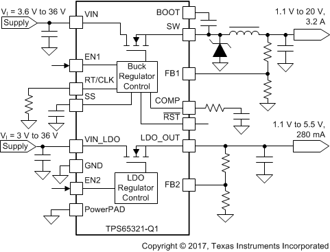
The TPS65321A-Q1 device is a combination of a high-VIN DC-DC step-down converter, referred to as the buck regulator, with an adjustable switch-mode frequency from 100-kHz to 2.5-MHz, and a high-VIN 280-mA low-dropout (LDO) regulator. The input range is 3.6 V to 36 V for the buck regulator, and 3 V to
36 V for the LDO regulator. The buck regulator has an integrated high-side MOSFET with an active-low, open-drain power-good output-pin (nRST). The LDO regulator features a low-input supply current of 45-μA typical in no-load, also has an integrated MOSFET. Low-voltage tracking feature enables TPS65321A-Q1 to track the input supply during cold-crank conditions.
The buck regulator provides a flexible design to fit system needs. The external loop compensation circuit allows for optimization of the converter response for the appropriate operating conditions. A low-ripple pulse-skip mode reduces the no-load input-supply current to maximum 140 μA.
The device has built-in protection features such as soft start, current-limit, thermal sensing and shutdown due to excessive power dissipation. Furthermore, the device has an internal undervoltage-lockout (UVLO) function that turns off the device when the supply voltage is too low.
Device Information(1)
| PART NUMBER | PACKAGE | BODY SIZE (NOM) |
|---|---|---|
| TPS65321A-Q1 | HTSSOP (14) | 5.00 mm × 4.40 mm |
- For all available packages, see the orderable addendum at the end of the data sheet.
Typical Application Schematic

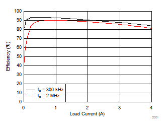
Buck Efficiency Versus Output Current
