ZHCSIX2 October 2018 TPS65216
PRODUCTION DATA.
- 1器件概述
- 2Pin Configuration and Functions
- 3Specifications
-
4Detailed Description
- 4.1 Overview
- 4.2 Functional Block Diagram
- 4.3
Feature Description
- 4.3.1
Wake-Up and Power-Up and Power-Down Sequencing
- 4.3.1.1 Power-Up Sequencing
- 4.3.1.2 Power-Down Sequencing
- 4.3.1.3 Strobes 1 and 2
- 4.3.1.4 Supply Voltage Supervisor and Power Good (PGOOD)
- 4.3.1.5 Internal LDO (INT_LDO)
- 4.3.1.6 Current Limited Load Switch
- 4.3.1.7 LDO1
- 4.3.1.8 UVLO
- 4.3.1.9 Power-Fail Comparator
- 4.3.1.10 DCDC3 / DCDC4 Power-Up Default Selection
- 4.3.1.11 I/O Configuration
- 4.3.1.12 Push Button Input (PB)
- 4.3.1.13 AC_DET Input (AC_DET)
- 4.3.1.14 Interrupt Pin (INT)
- 4.3.1.15 I2C Bus Operation
- 4.3.1
Wake-Up and Power-Up and Power-Down Sequencing
- 4.4 Device Functional Modes
- 4.5
Register Maps
- 4.5.1 Password Protection
- 4.5.2 FLAG Register
- 4.5.3
TPS65216Registers
- 4.5.3.1 CHIPID Register (subaddress = 0x0) [reset = 0x5]
- 4.5.3.2 INT1 Register (subaddress = 0x1) [reset = 0x0]
- 4.5.3.3 INT2 Register (subaddress = 0x2) [reset = 0x0]
- 4.5.3.4 INT_MASK1 Register (subaddress = 0x3) [reset = 0x0]
- 4.5.3.5 INT_MASK2 Register (subaddress = 0x4) [reset = 0x0]
- 4.5.3.6 STATUS Register (subaddress = 0x5) [reset = 00XXXXXXb]
- 4.5.3.7 CONTROL Register (subaddress = 0x6) [reset = 0x0]
- 4.5.3.8 FLAG Register (subaddress = 0x7) [reset = 0x0]
- 4.5.3.9 PASSWORD Register (subaddress = 0x10) [reset = 0x0]
- 4.5.3.10 ENABLE1 Register (subaddress = 0x11) [reset = 0x0]
- 4.5.3.11 ENABLE2 Register (subaddress = 0x12) [reset = 0x0]
- 4.5.3.12 CONFIG1 Register (subaddress = 0x13) [reset = 0x4C]
- 4.5.3.13 CONFIG2 Register (subaddress = 0x14) [reset = 0xC0]
- 4.5.3.14 CONFIG3 Register (subaddress = 0x15) [reset = 0x0]
- 4.5.3.15 DCDC1 Register (offset = 0x16) [reset = 0x99]
- 4.5.3.16 DCDC2 Register (subaddress = 0x17) [reset = 0x99]
- 4.5.3.17 DCDC3 Register (subaddress = 0x18) [reset = 0x8C]
- 4.5.3.18 DCDC4 Register (subaddress = 0x19) [reset = 0xB2]
- 4.5.3.19 SLEW Register (subaddress = 0x1A) [reset = 0x6]
- 4.5.3.20 LDO1 Register (subaddress = 0x1B) [reset = 0x1F]
- 4.5.3.21 SEQ1 Register (subaddress = 0x20) [reset = 0x0]
- 4.5.3.22 SEQ2 Register (subaddress = 0x21) [reset = 0x0]
- 4.5.3.23 SEQ3 Register (subaddress = 0x22) [reset = 0x98]
- 4.5.3.24 SEQ4 Register (subaddress = 0x23) [reset = 0x75]
- 4.5.3.25 SEQ5 Register (subaddress = 0x24) [reset = 0x12]
- 4.5.3.26 SEQ6 Register (subaddress = 0x25) [reset = 0x63]
- 4.5.3.27 SEQ7 Register (subaddress = 0x26) [reset = 0x3]
- 5Application and Implementation
- 6Power Supply Recommendations
- 7Layout
- 8器件和文档支持
- 9机械、封装和可订购信息
4.3.1.4 Supply Voltage Supervisor and Power Good (PGOOD)
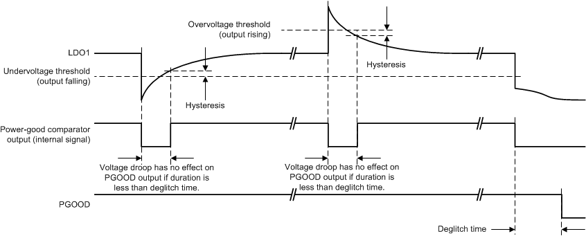
Power-good (PGOOD) is an open-drain output of the built-in voltage supervisor that monitors DCDC1, DCDC2, DCDC3, DCDC4, and LDO1. The output is Hi-Z when all enabled rails are in regulation and driven low when one or more rails encounter a fault which brings the output voltage outside the specified tolerance range. In a typical application PGOOD drives the reset signal of the SOC.
The supervisor has two modes of operation, controlled by the STRICT bit. With the STRICT bit set to 0, all enabled rails of the five regulators are monitored for undervoltage only with relaxed thresholds and deglitch times. With the STRCT bit set to 1, all enabled rails of the five regulators are monitored for undervoltage and overvoltage with tight limits and short deglitch times. Table 4-1 summarizes these details.
Table 4-1 Supervisor Characteristics Controlled by the STRICT Bit
| PARAMETER | STRICT = 0b (TYP) | STRICT = 1b (TYP) | |
|---|---|---|---|
| Undervoltage monitoring | Threshold (output falling) | 90% | 96.5% (DCDC1, DCDC2)
95.5% (DCDC3, DCDC4, LDO1) |
| Deglitch (output falling) | 1 ms | 50 µs | |
| Deglitch (output rising) | 10 µs | 10 µs | |
| Overvoltage monitoring | Threshold (output falling) | N/A | 103.5% (DCDC1, DCDC2)
104.5% (DCDC3, DCDC4, LDO1) |
| Deglitch (output falling) | N/A | 1 ms | |
| Deglitch (output rising) | N/A | 50 µs | |
 Figure 4-7 Definition of Undervoltage, Overvoltage Thresholds, Hysteresis, and Deglitch Times
 The following rules apply to the PGOOD output:
- The power-up default state for PGOOD is low. When all rails are disabled, PGOOD output is driven low.
- Only enabled rails are monitored. Disabled rails are ignored.
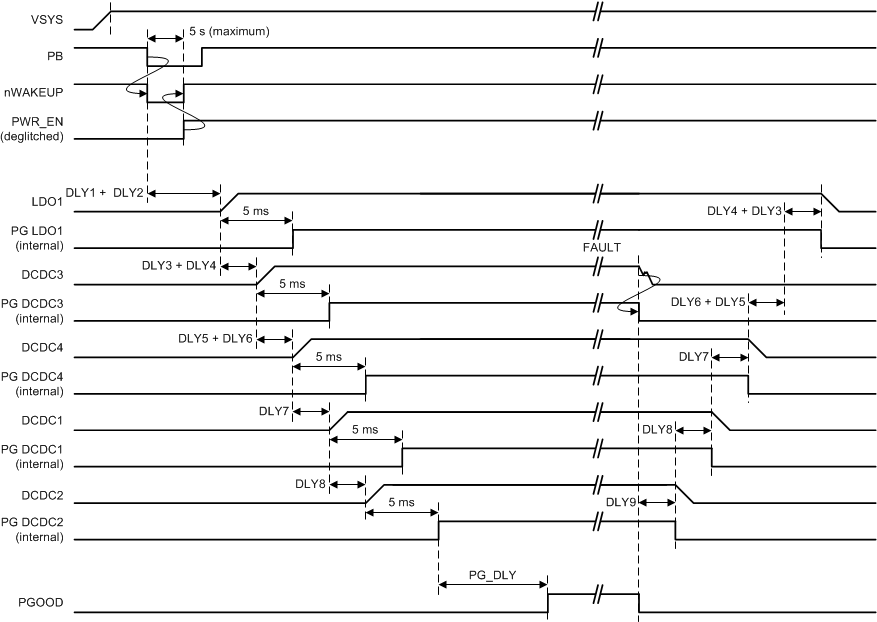
- Power-good monitoring of a particular rail starts 5 ms after the rail is enabled and is continuously monitored thereafter. This allows the rail to power-up.
- PGOOD is delayed by PGDLY time after the sequencer is finished and the last rail is enabled.
- If an enabled rail is continuously outside the monitoring threshold for longer than the deglitch time, PGOOD is pulled low, and all rails are shut-down following the power-down sequence. PGDLY does not apply.
- Disabling a rail manually by resetting the DCx_EN or LDO1_EN bit has no effect on the PGOOD pin. If all rails are disabled, PGOOD is driven low as the last rail is disabled.
- If the power-down sequencer is triggered, PGOOD is driven low.
- PGOOD is driven low in SUSPEND state, regardless of the number of rails that are enabled.
Figure 4-8 shows a typical power-up sequence and PGOOD timing.
 Figure 4-8 Typical Power-Up Sequence of the Main Output Rails