ZHCSQI6C May   2022  – October 2023 TPS62870-Q1 , TPS62871-Q1 , TPS62872-Q1 , TPS62873-Q1

PRODUCTION DATA  

  1.   1
  2. 特性
  3. 应用
  4. 说明
  5. Revision History
  6. 说明(续)
  7. Device Options
  8. Pin Configuration and Functions
  9. Specifications
    1. 8.1 Absolute Maximum Ratings
    2. 8.2 ESD Ratings
    3. 8.3 Recommended Operating Conditions
    4. 8.4 Thermal Information
    5. 8.5 Electrical Characteristics
    6. 8.6 I2C Interface Timing Characteristics
    7. 8.7 Timing Requirements
    8. 8.8 Typical Characteristics
  10. Detailed Description
    1. 9.1 Overview
    2. 9.2 Functional Block Diagram
    3. 9.3 Feature Description
      1. 9.3.1  Fixed-Frequency DCS Control Topology
      2. 9.3.2  Forced PWM and Power Save Modes
      3. 9.3.3  Precise Enable
      4. 9.3.4  Start-Up
      5. 9.3.5  Switching Frequency Selection
      6. 9.3.6  Output Voltage Setting
        1. 9.3.6.1 Output Voltage Range
        2. 9.3.6.2 Output Voltage Setpoint
        3. 9.3.6.3 Non-Default Output Voltage Setpoint
        4. 9.3.6.4 Dynamic Voltage Scaling
      7. 9.3.7  Compensation (COMP)
      8. 9.3.8  Mode Selection and Clock Synchronization (MODE/SYNC)
      9. 9.3.9  Spread Spectrum Clocking (SSC)
      10. 9.3.10 Output Discharge
      11. 9.3.11 Undervoltage Lockout (UVLO)
      12. 9.3.12 Overvoltage Lockout (OVLO)
      13. 9.3.13 Overcurrent Protection
        1. 9.3.13.1 Cycle-by-Cycle Current Limiting
        2. 9.3.13.2 Hiccup Mode
        3. 9.3.13.3 Current Limit Mode
      14. 9.3.14 Power Good (PG)
        1. 9.3.14.1 Standalone or Primary Device Behavior
        2. 9.3.14.2 Secondary Device Behavior
      15. 9.3.15 Remote Sense
      16. 9.3.16 Thermal Warning and Shutdown
      17. 9.3.17 Stacked Operation
    4. 9.4 Device Functional Modes
      1. 9.4.1 Power-On Reset
      2. 9.4.2 Undervoltage Lockout
      3. 9.4.3 Standby
      4. 9.4.4 On
    5. 9.5 Programming
      1. 9.5.1 Serial Interface Description
      2. 9.5.2 Standard, Fast, Fast Mode Plus Protocol
      3. 9.5.3 I2C Update Sequence
      4. 9.5.4 I2C Register Reset
    6. 9.6 Register Map
  11. 10Application and Implementation
    1. 10.1 Application Information
    2. 10.2 Typical Application
      1. 10.2.1 Design Requirements
      2. 10.2.2 Detailed Design Procedure
        1. 10.2.2.1 Selecting the Inductor
        2. 10.2.2.2 Selecting the Input Capacitors
        3. 10.2.2.3 Selecting the Compensation Resistor
        4. 10.2.2.4 Selecting the Output Capacitors
        5. 10.2.2.5 Selecting the Compensation Capacitor, CC
        6. 10.2.2.6 Selecting the Compensation Capacitor, CC2
      3. 10.2.3 Application Curves
    3. 10.3 Best Design Practices
    4. 10.4 Power Supply Recommendations
    5. 10.5 Layout
      1. 10.5.1 Layout Guidelines
      2. 10.5.2 Layout Example
  12. 11Device and Documentation Support
    1. 11.1 Device Support
      1. 11.1.1 第三方产品免责声明
    2. 11.2 Documentation Support
      1. 11.2.1 Related Documentation
    3. 11.3 接收文档更新通知
    4. 11.4 支持资源
    5. 11.5 Trademarks
    6. 11.6 静电放电警告
    7. 11.7 术语表
  13. 12Mechanical, Packaging, and Orderable Information

封装选项

机械数据 (封装 | 引脚)
散热焊盘机械数据 (封装 | 引脚)
订购信息

Cycle-by-Cycle Current Limiting

If the peak inductor current increases above the high-side current limit threshold, the device turns off the high-side switch and turns on the low-side switch to ramp down the inductor current. The device only turns on the high-side switch again if the inductor current has decreased below the low-side current limit threshold.

Note that because of the propagation delay of the current limit comparator, the current limit threshold in practice can be greater than the DC value specified in the Electrical Characteristics. The current limit in practice is given by:
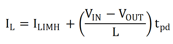
Equation 3.
GUID-C1D23215-BCF3-412F-95EA-AA93DF78D166-low.gif

where:

  • IL is the inductor current.
  • ILIMH is the high-side current limit threshold measured at DC.
  • VIN is the input voltage.
  • VOUT is the output voltage.
  • L is the effective inductance at the peak current level.
  • tpd is the propagation delay of the current limit comparator (typically 50 ns).