ZHCS342B November   2013  – July 2014 TPS62740 , TPS62742

PRODUCTION DATA.  

  1. 特性
  2. 应用范围
  3. 说明
  4. 典型应用
  5. 修订历史记录
  6. Device Comparison Table
  7. Pin Configuration and Functions
  8. Specifications
    1. 8.1 Absolute Maximum Ratings
    2. 8.2 Handling Ratings
    3. 8.3 Recommended Operating Conditions
    4. 8.4 Thermal Information
    5. 8.5 Electrical Characteristics
    6. 8.6 Typical Characteristics
  9. Detailed Description
    1. 9.1 Overview
    2. 9.2 Functional Block Diagram
    3. 9.3 Feature Description
      1. 9.3.1 DCS-Control™
      2. 9.3.2 CTRL / Output Load
      3. 9.3.3 Enable / Shutdown
      4. 9.3.4 Power Good Output (PG)
      5. 9.3.5 Output Voltage Selection (VSEL1 - 4)
      6. 9.3.6 Softstart
      7. 9.3.7 Undervoltage Lockout UVLO
    4. 9.4 Device Functional Modes
      1. 9.4.1 VOUT And LOAD Output Discharge
      2. 9.4.2 Automatic Transition Into 100% Mode
      3. 9.4.3 Internal Current Limit
      4. 9.4.4 Dynamic Voltage Scaling with VSEL Interface
  10. 10Application and Implementation
    1. 10.1 Application Information
    2. 10.2 Typical Application
      1. 10.2.1 Design Requirements
      2. 10.2.2 Detailed Design Procedure
        1. 10.2.2.1 Inductor Selection
        2. 10.2.2.2 DC/DC Output Capacitor Selection
        3. 10.2.2.3 Input Capacitor Selection
      3. 10.2.3 Application Curves
    3. 10.3 System Example
  11. 11Power Supply Recommendations
  12. 12Layout
    1. 12.1 Layout Guidelines
    2. 12.2 Layout Example
  13. 13器件和文档支持
    1. 13.1 器件支持
      1. 13.1.1 第三方产品免责声明
    2. 13.2 文档支持
      1. 13.2.1 相关文档 
    3. 13.3 相关链接
    4. 13.4 商标
    5. 13.5 静电放电警告
    6. 13.6 术语表
  14. 14机械封装和可订购信息

封装选项

机械数据 (封装 | 引脚)
散热焊盘机械数据 (封装 | 引脚)
订购信息

10 Application and Implementation

10.1 Application Information

The TPS6274x devices are a step down converter family featuring typ. 360nA quiescent current and operating with a tiny 2.2µH inductor and 10µF output capacitor. This new DCS-ControlTM based devices extend the light load efficiency range below 10µA load currents. TPS62740 supports output currents up to 300mA, TPS62742 up to 400mA. The devices operate from rechargeable Li-Ion batteries, Li-primary battery chemistries such as Li-SOCl2, Li-MnO2 and two or three cell alkaline batteries.

10.2 Typical Application

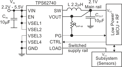
TPS62740 TPS62742 TPS62740_12pin_2.1V_app_drw.gifFigure 7. TPS62740 Typical Application Circuit
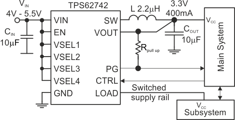
TPS62740 TPS62742 TPS62742_12pin_3.3V_app_drw_nest.gifFigure 8. TPS62742 Typical Application Circuit

10.2.1 Design Requirements

The TPS6274x is a highly integrated DC/DC converter. The output voltage is set via a VSEL pin interface without any additional external components. For proper operation only a input- and output capacitor and an inductor is required. The integrated load switch doesn't require a capacitor on its LOAD pin. Table 2 shows the components used for the application characteristic curves.

Table 2. Components for Application Characteristic Curves

Reference Description Value Manufacturer
TPS62740/42 360nA Iq step down converter Texas Instruments
CIN, COUT, CLOAD Ceramic capacitor GRM188R60J106M 10µF Murata
L Inductor LPS3314 2.2µH Coilcraft

10.2.2 Detailed Design Procedure

Table 3 shows the recommended output filter components. The TPS6274x is optimized for operation with a 2.2µH inductor and with 10µF output capacitor.

Table 3. Recommended LC Output Filter Combinations

Inductor Value [µH](2) Output Capacitor Value [µF](1)
4.7µF 10µF 22µF
2.2 (3)
(1) Capacitance tolerance and bias voltage de-rating is anticipated. The effective capacitance can vary by 20% and -50%.
(2) Inductor tolerance and current de-rating is anticipated. The effective inductance can vary by 20% and -30%.
(3) This LC combination is the standard value and recommended for most applications.

10.2.2.1 Inductor Selection

The inductor value affects its peak-to-peak ripple current, the PWM-to-PFM transition point, the output voltage ripple and the efficiency. The selected inductor has to be rated for its DC resistance and saturation current. The inductor ripple current (ΔIL) decreases with higher inductance and increases with higher VIN or VOUT and can be estimated according to Equation 1.

Equation 2 calculates the maximum inductor current under static load conditions. The saturation current of the inductor should be rated higher than the maximum inductor current, as calculated with Equation 2. This is recommended because during a heavy load transient the inductor current rises above the calculated value. A more conservative way is to select the inductor saturation current above the high-side MOSFET switch current limit, ILIMF.

Equation 1. TPS62740 TPS62742 eq4_dil_lvs941.gif
Equation 2. TPS62740 TPS62742 eq5_ilmax_lvs941.gif

With:

f = Switching Frequency
L = Inductor Value
ΔIL= Peak to Peak inductor ripple current
ILmax = Maximum Inductor current

In DC/DC converter applications, the efficiency is essentially affected by the inductor AC resistance (i.e. quality factor) and by the inductor DCR value. Increasing the inductor value produces lower RMS currents, but degrades transient response. For a given physical inductor size, increased inductance usually results in an inductor with lower saturation current.

The total losses of the coil consist of both the losses in the DC resistance (RDC) and the following frequency-dependent components:

  • The losses in the core material (magnetic hysteresis loss, especially at high switching frequencies)
  • Additional losses in the conductor from the skin effect (current displacement at high frequencies)
  • Magnetic field losses of the neighboring windings (proximity effect)
  • Radiation losses

The following inductor series from different suppliers have been used:

Table 4. List Of Inductors(1)

INDUCTANCE [µH] DIMENSIONS [mm3] INDUCTOR TYPE SUPPLIER
2.2 3.3 x 3.3 x 1.4 LPS3314 Coilcraft
2.2 2.5 x 3.0 x 1.5 VLF302515MT TDK
2.2 2.0 × 1.2 × 1.0 MIPSZ2012 2R2 FDK
2.2 2.5 x 2.0 x 1.2 MIPSA2520 2R2 FDK
2.2 2.0 x 1.2 x 1.0 MDT2012CH2R2 TOKO

10.2.2.2 DC/DC Output Capacitor Selection

The DCS-Control™ scheme of the TPS6274x allows the use of tiny ceramic capacitors. Ceramic capacitors with low ESR values have the lowest output voltage ripple and are recommended. The output capacitor requires either an X7R or X5R dielectric. Y5V and Z5U dielectric capacitors, aside from their wide variation in capacitance over temperature, become resistive at high frequencies. At light load currents, the converter operates in Power Save Mode and the output voltage ripple is dependent on the output capacitor value and the PFM peak inductor current. A larger output capacitors can be used, but it should be considered that larger output capacitors lead to an increased leakage current in the capacitor and may reduce overall conversion efficiency. Furthermore, larger output capacitors impact the start up behavior of the DC/DC converter.
10.2.2.3 Input Capacitor Selection

Because the buck converter has a pulsating input current, a low ESR input capacitor is required for best input voltage filtering to ensure proper function of the device and to minimize input voltage spikes. For most applications a 10µF is sufficient. The input capacitor can be increased without any limit for better input voltage filtering.

Table 5 shows a list of tested input/output capacitors.

Table 5. List Of Capacitors(1)

CAPACITANCE [μF] SIZE CAPACITOR TYPE SUPPLIER
10 0603 GRM188R60J106ME84 Murata

10.2.3 Application Curves

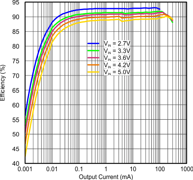
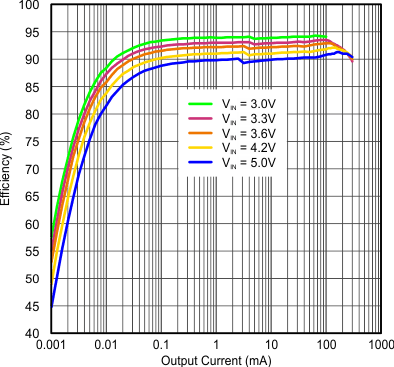
TPS62740 TPS62742 eff_vs_IO_1.8V_LPS3314_2R2.gif
COUT = 10 µF (0603) CTRL = GND
L = 2.2 µH (LPS3314 2R2)
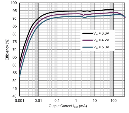
Figure 9. Efficiency VOUT = 1.8V
TPS62740 TPS62742 eff_vs_IOUT_VO_3_3V_TPS62742_VLF302515_2R2.gif
COUT = 10 µF, CTRL = GND.
L = 2.2 µH (VLF302515)
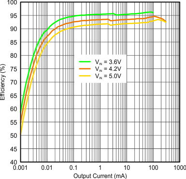
Figure 11. Efficiency VOUT = 3.3V TPS62742
TPS62740 TPS62742 eff_vs_IOUT_VO_3_3V_LPS3314_2R2.gif
COUT = 10 µF (0603) CTRL = GND
L = 2.2 µH (LPS3314 2R2)
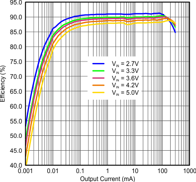
Figure 13. Efficiency VOUT = 3.3V
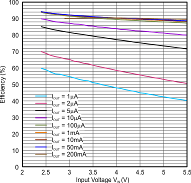
TPS62740 TPS62742 eff_vs_VIN_VO_2.1V_LPS3314_2R2.gif
COUT = 10 µF (0603) CTRL = GND
L = 2.2 µH (LPS3314 2R2)
Figure 15. Efficiency VOUT = 2.1V
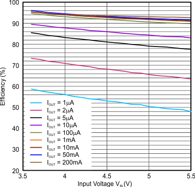
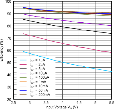
TPS62740 TPS62742 eff_vs_VIN_VO_3.3V_LPS3314_2R2.gif
COUT = 10 µF (0603) CTRL = GND
L = 2.2 µH (LPS3314 2R2)
Figure 17. Efficiency VOUT = 3.3V
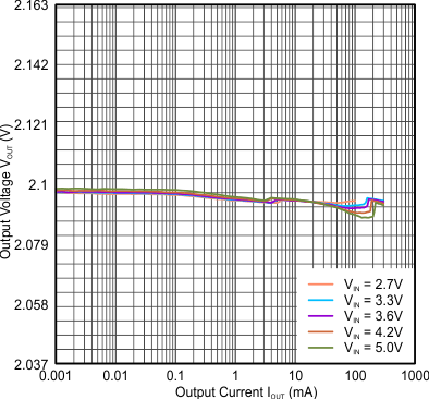
TPS62740 TPS62742 VO_accuracy_2_1V_25C.gif
COUT = 10 µF (0603) CTRL = GND
L = 2.2 µH (LPS3314 2R2)
Figure 19. Output Voltage VOUT = 2.1V
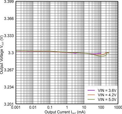
TPS62740 TPS62742 VO_accuracy_3_3V_25C.gif
COUT = 10 µF (0603) CTRL = GND
L = 2.2 µH (LPS3314 2R2)
Figure 21. Output Voltage VOUT = 3.3V
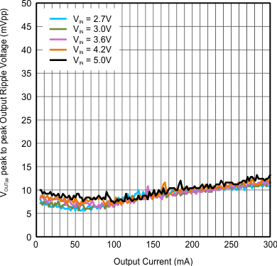
TPS62740 TPS62742 VOPP_VO1_8V_Vs_IO_VS_VIN.gif
COUT = 10 µF (0603) CTRL = GND
L = 2.2 µH
Figure 23. Typical Output Ripple Voltage VOUT = 1.8V
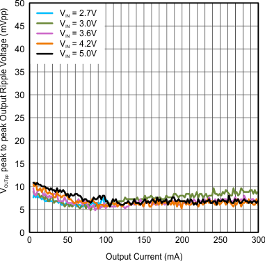
TPS62740 TPS62742 VOPP_VO2_1V_Vs_IO_VS_VIN.gif
COUT = 10 µF (0603) CTRL = GND
L = 2.2 µH
Figure 25. Typical Output Ripple Voltage VOUT = 2.1V
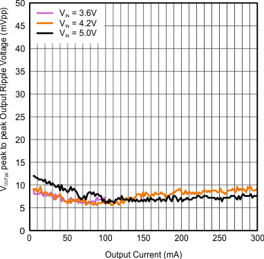
TPS62740 TPS62742 VOPP_VO3_0V_Vs_IO_VS_VIN.gif
COUT = 10 µF (0603) CTRL = GND
L = 2.2 µH
Figure 27. Typical Output Ripple Voltage VOUT = 3.0V
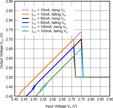
TPS62740 TPS62742 100_mode_2_5V_VOUT.gif
L = 2.2 µH (LPS3314)
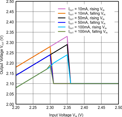
Figure 29. 100% Mode Transition VOUT 2.5V
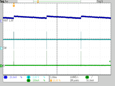
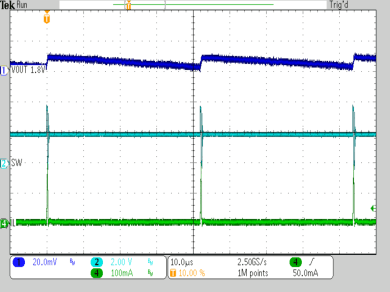
TPS62740 TPS62742 SP_TO_3V6_1V8_10uA_2uH2_10uF.gif
VIN = 3.6 V IOUT = 10 µA L = 2.2 µH
COUT = 10 µF CTRL = GND
Figure 31. Typical Operation ILoad = 10µA VOUT = 1.8V
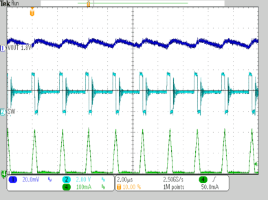
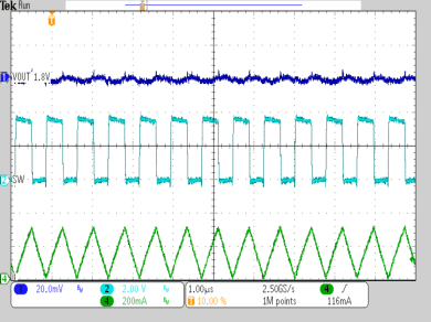
TPS62740 TPS62742 SP_TO_3V6_1V8_25mA_2uH2_10uF.gif
VIN = 3.6 V IOUT = 25 mA L = 2.2 µH
COUT = 10 µF CTRL = GND
Figure 33. Typical Operation ILoad = 25mA, VOUT = 1.8V
TPS62740 TPS62742 SP_LTR_3V6_1V8_50uA_to_t10mA_CTRL-GND_L_2uH2_CO_10uF.gif
VIN = 3.6 V IOUT = 50 µA to 10 mA L = 2.2 µH
COUT = 10 µF CTRL = GND
Figure 35. Load Transient Response VOUT = 1.8V
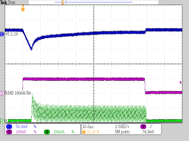
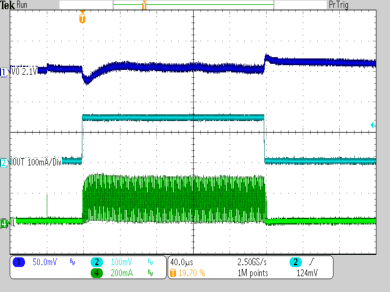
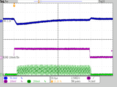
TPS62740 TPS62742 transient_response_out_of_sleep.gif
VIN = 3.6 V, VOUT = 2.1 V L = 2.2 µH COUT = 10 µF
Loadstep at VOUT 0 mA to 100 mA,
1 µs rise/ fall time, 70 µs / 7 ms
Figure 37. Load Transient Response CTRL = GND
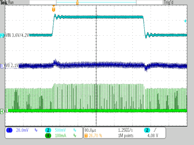
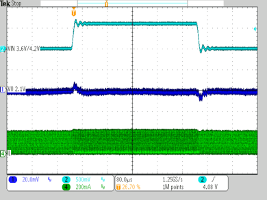
TPS62740 TPS62742 SP_LineTranient_3V6_4_2V_VO_2.1V_10mA_CTRL-GND_L_2uH2_CO_10uF.gif
VIN = 3.6 V / 4.2 V VOUT = 2.1 V L = 2.2 µH
COUT = 10 µF CTRL = GND
Figure 39. Line Transient Response IOUT=10mA
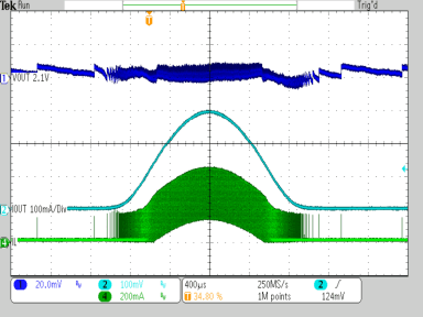
TPS62740 TPS62742 SP_AC_load_sweep_3V6_2V1_50uA_to_300mA_CTRL-GND_L_2uH2_CO_10uF.gif
VIN = 3.6 V IOUT = 50 µA to 300 mA L = 2.2 µH
COUT = 10 µF CTRL = GND
Figure 41. AC Load Sweep VOUT = 2.1V
TPS62740 TPS62742 SP_VLoad_discharge_3V6_2V1_L_2uH2_CO_10uF.gif
VIN = 3.6 V VOUT = 2.1 V ILOAD = 0 mA
IOUT = 0 mA COUT = 10 µF CLOAD = 10 µF
L = 2.2 µH
Figure 43. Load Output On / Off
TPS62740 TPS62742 SP_VOUT_ramp_up_CTRL_GND_3V6_2V1_L_2uH2_CO_10uF.gif
VIN = 3.6 V VOUT = 2.1 V CTRL = GND
ROUT = 100 Ω COUT = 10 µF L = 2.2 µH
Figure 45. VOUT Ramp Up After Enable
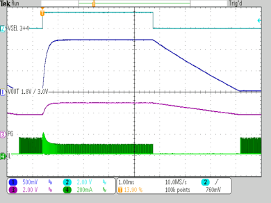
TPS62740 TPS62742 SP_DVS_1V8_3V_0_CTRL_GND_5mA_IOUT_3V6_2V1_L_2uH2_CO_10uF.gif
VIN = 3.6 V Ramp up / Down
COUT = 10 µF CTRL = GND VSEL 3+4 toggled
IOUT = 5 mA L = 2.2 µH VSEL 1+2 = GND
Figure 47. Dynamic Output Voltage Scaling
VOUT = 1.8V/3.0V
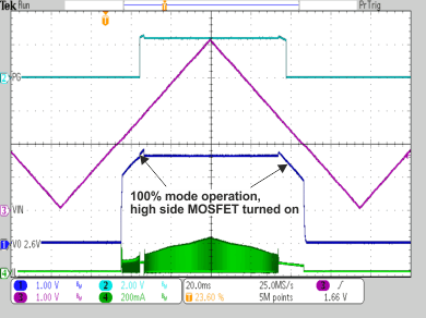
TPS62740 TPS62742 VIN_ramp_up_down_VO_2V6_50R_CTRL_gnd.gif
COUT = 10 µF L = 2.2 µH CTRL = GND
VIN = ramp up/down 0 V to 5 V, 150 ms,
Output resistance 50 Ω
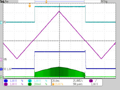
Figure 49. Input Voltage Ramp Up/Down VOUT = 2.6V
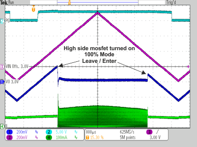
TPS62740 TPS62742 100_mode_transition_VO_3V0_50R.gif
VOUT = 3.0 V COUT = 10 µF L = 2.2 µH, CTRL = GND
VIN = ramp up /down 2.8 V to 3.7 V,
Output resistance 50 Ω
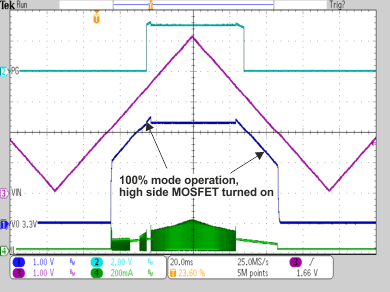
Figure 51. Enter/Leave 100% Mode Operation
TPS62740 TPS62742 eff_vs_IOUT_VO2_1V_LPS3314_2R2.gif
COUT = 10 µF (0603) CTRL = GND
L = 2.2 μH (LPS3314 2R2)
Figure 10. Efficiency VOUT = 2.1V
TPS62740 TPS62742 eff_vs_IOUT_VO2_5V_LPS3314_2R2.gif
COUT = 10 µF (0603) CTRL = GND
L = 2.2 µH (LPS3314 2R2)
Figure 12. Efficiency VOUT = 2.5V
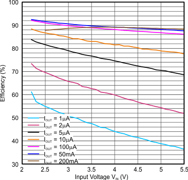
TPS62740 TPS62742 eff_vs_VIN_VO_1_8V_LPS3314_2R2.gif
COUT = 10 µF (0603) CTRL = GND
L = 2.2 µH (LPS3314 2R2)
Figure 14. Efficiency VOUT = 1.8V
TPS62740 TPS62742 eff_vs_VIN_VO_2.5V_LPS3314_2R2.gif
COUT = 10 µF (0603) CTRL = GND
L = 2.2 µH (LPS3314 2R2)
Figure 16. Efficiency VOUT = 2.5V
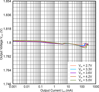
TPS62740 TPS62742 VO_accuracy_1.8V_25C.gif
COUT = 10 µF (0603) CTRL = GND
L = 2.2 µH (LPS3314 2R2)
Figure 18. Output Voltage VOUT = 1.8V
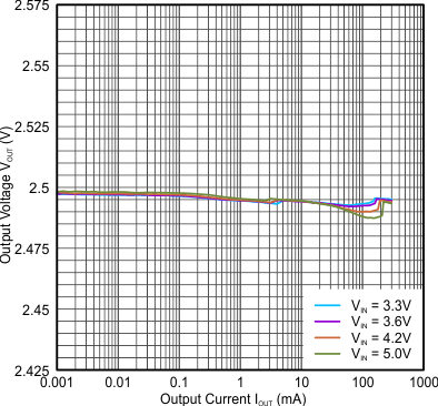
TPS62740 TPS62742 VO_accuracy_2_5V_25C.gif
COUT = 10 µF (0603) CTRL = GND
L = 2.2 µH (LPS3314 2R2)
Figure 20. Output Voltage VOUT = 2.5V
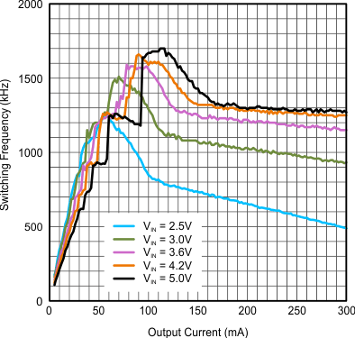
TPS62740 TPS62742 fsw_vs_IO_vs_VIN_VO_1p8V.gif
COUT = 10 µF L = 2.2 µH
Figure 22. Typical Switching Frequency VOUT = 1.8V
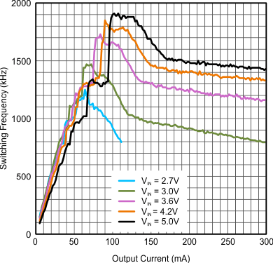
TPS62740 TPS62742 fsw_vs_IO_vs_VIN_VO_2p1V.gif
COUT = 10 µF L = 2.2 µH
Figure 24. Typical Switching Frequency VOUT = 2.1V
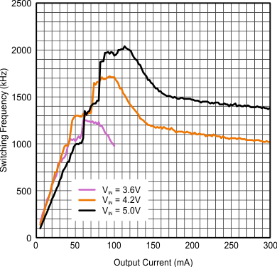
TPS62740 TPS62742 fsw_vs_IO_vs_VIN_VO_3p0V.gif
COUT = 10 µF L = 2.2 µH
Figure 26. Typical Switching Frequency VOUT = 3.0V
TPS62740 TPS62742 100_mode_2_1V_VOUT.gif
L = 2.2 µH (LPS3314)
Figure 28. 100% Mode Transition VOUT 2.1V
TPS62740 TPS62742 100_mode_3_3V_VOUT.gif
L = 2.2 µH (LPS3314)
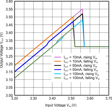
Figure 30. 100% Mode Transition VOUT 3.3V
TPS62740 TPS62742 SP_TO_3V6_1V8_1mA_2uH2_10uF.gif
VIN = 3.6 V IOUT = 1 mA L = 2.2 µH
COUT = 10 µF CTRL = GND
Figure 32. Typical Operation ILoad = 1ma, VOUT = 1.8V
TPS62740 TPS62742 SP_TO_3V6_1V8_150mA_2uH2_10uF.gif
VIN = 3.6 V IOUT = 150 mA L = 2.2 µH
COUT = 10 µF CTRL = GND
Figure 34. Typical Operation ILoad = 150ma, VOUT = 1.8V
TPS62740 TPS62742 SP_LTR_3V6_2V1_0_5mA_to_150mA_CTRL-VIN_L_2uH2_CO_10uF.gif
VIN = 3.6 V IOUT = 0.5 mA to 150 mA L = 2.2 µH
COUT = 10 µF CTRL = VIN
Figure 36. Load Transient Response VOUT = 2.1V
TPS62740 TPS62742 transient_response_out_of_PFM_active.gif
VIN = 3.6 V, VOUT = 2.1 V L = 2.2 µH, COUT = 10 µF
Loadstep at VOUT 0 mA to 100 mA,
1 µs rise/fall time; 70 µs / 7 ms
Figure 38. Load Transient Response CTRL = VIN
TPS62740 TPS62742 SP_LineTranient_3V6_4_2V_VO_2.1V_100mA_CTRL-GND_L_2uH2_CO_10uF.gif
VIN = 3.6 V / 4.2 V VOUT = 2.1 V L = 2.2 µH
COUT = 10 µF CTRL = GND
Figure 40. Line Transient Response IOUT = 100mA
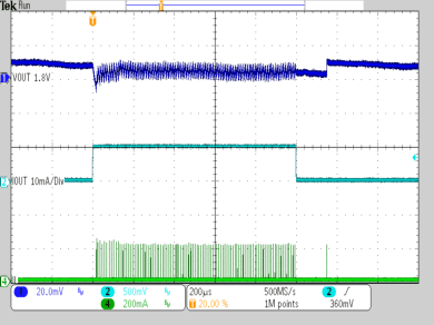
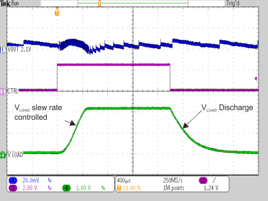
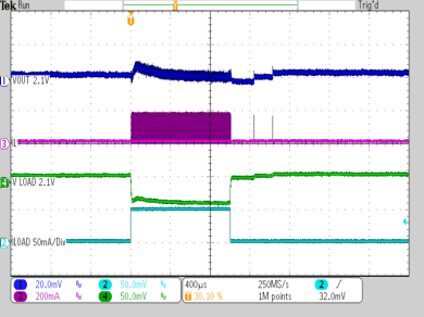
TPS62740 TPS62742 SP_VLOAD_loadstep_50mA_CTRL_VIN_3V6_2V1_L_2uH2_CO_10uF.gif
VIN = 3.6 V, VOUT = VLOAD= 2.1 V CTRL = VIN
IOUT = 0 mA CLOAD = 10 µF L = 2.2 µH
COUT = 10 µF ILOAD = 0 to 50 mA to 0 mA
Figure 42. Load Step At Load Output
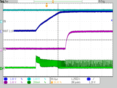
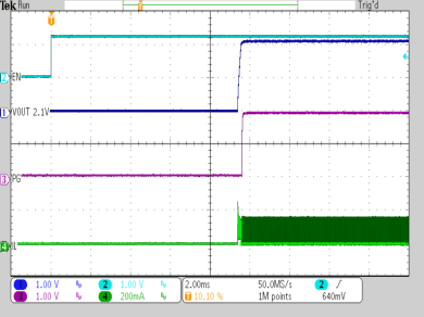
TPS62740 TPS62742 SP_VOUT_startup_3V6_2V1_L_2uH2_CO_10uF_CTRL_gnd.gif
VIN = 3.6 V VOUT = 2.1 V CTRL = GND
ROUT = 100 Ω COUT = 10 µF L = 2.2 µH
Figure 44. Device Enable And Start Up
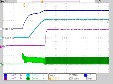
TPS62740 TPS62742 SP_VOUT_VLOAD_ramp_up_CTRL_high_100R_ROUT_3V6_2V1_L_2uH2_CO_10uF.gif
VIN = 3.6 V VOUT = VLOAD = 2.1 V CTRL = VIN
ROUT = 100 Ω, COUT = CLOAD = 10 µF L = 2.2 µH
ILOAD = 0 mA
Figure 46. VOUT Ramp Up With Activated Load Switch
TPS62740 TPS62742 VIN_ramp_up_down_VO_1V8_50R_CTRL_gnd.gif
COUT = 10 µF L = 2.2 µH CTRL = GND
VIN = ramp up/down 0 V to 5 V, 150 ms,
Output resistance 50 Ω
Figure 48. Input Voltage Ramp Up/Down
VOUT = 1.8V
TPS62740 TPS62742 VIN_ramp_up_down_VO_3V3_50R_CTRL_gnd.gif
COUT = 10 µF L = 2.2 µH CTRL = GND
VIN = ramp up/down 0 V to 5 V, 150 ms,
Output resistance 50 Ω
Figure 50. Input Voltage Ramp Up/Down VOUT = 3.3V

10.3 System Example

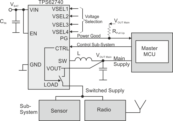
TPS62740 TPS62742 system_overview_master_mcu_12pin.gifFigure 52. Example Of Implementation In A Master MCU Based System