SLVSBO4C October 2012 – December 2014 TPS62736 , TPS62737
UNLESS OTHERWISE NOTED, this document contains PRODUCTION DATA.
- 1 Features
- 2 Applications
- 3 Description
- 4 Revision History
- 5 Description (continued)
- 6 Device Voltage Options
- 7 Pin Configuration and Functions
- 8 Specifications
- 9 Detailed Description
- 10Application and Implementation
- 11Power Supply Recommendations
- 12Layout
- 13Device and Documentation Support
- 14Mechanical, Packaging, and Orderable Information
9 Detailed Description
9.1 Overview
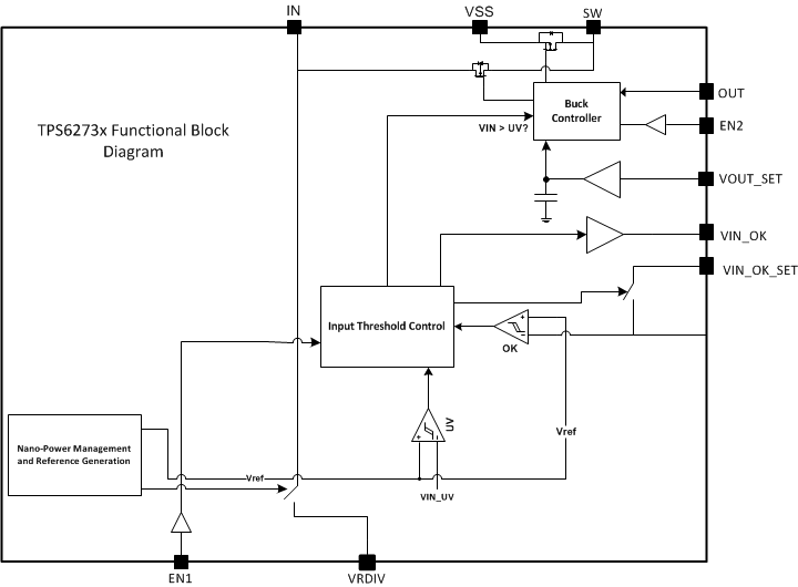
The TPS6273x family provides a highly integrated ultra low power buck converter solution that is well suited for meeting the special needs of ultra-low power applications such as energy harvesting. The TPS6273x provides the system with an externally programmable regulated supply in order to preserve the overall efficiency of the power-management stage compared to a linear step down converter. This regulator is intended to step-down the voltage from an energy storage element such as a battery or super capacitor in order to supply the rail to low-voltage electronics. The regulated output has been optimized to provide high efficiency across low-output currents (<10 µA) to high currents (200 mA).
The TPS6273x integrates an optimized hysteretic controller for low-power applications. The internal circuitry uses a time-based sampling system to reduce the average quiescent current.
9.2 Functional Block Diagram
9.3 Feature Description
9.3.1 Step-Down (Buck) Converter Operation
The buck regulator in the TPS6273x takes input power from VIN, steps it down and provides a regulated voltage at the OUT pin. It employs pulse frequency modulation (PFM) control to regulate the voltage close to the desired reference voltage. The reference voltage is set by the user programmed resistor divider. The current through the inductor is controlled through internal current sense circuitry. The peak current in the inductor is controlled to maintain high efficiency of the converter across a wide input current range. The TPS62736 converter delivers an average output current of 50mA with a peak inductor current of 100 mA. The TPS62737 converter delivers an average output current of 200 mA with a peak inductor current of 370 mA. The buck regulator is disabled when the voltage on VIN reaches the UVLO condition. The UVLO level is continuously monitored. The buck regulator continues to operate in pass (100% duty cycle) mode, passing the input voltage to the output, as long as VIN is greater than UVLO and less than VIN minus IOUT times RDS(on) of the high-side FET (that is, VIN – IOUT x RDS(on)-HS). In order to save power from being dissipated through other ICs on this supply rail while allowing for a faster wake up time, the buck regulator can be enabled and disabled through the EN2 pin for systems that desire to completely turn off the regulated output.
9.3.2 Programming OUT Regulation Voltage and VIN_OK
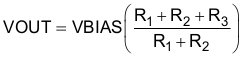
To set the proper output-regulation voltage and input voltage power-good comparator, the external resistors must be carefully selected. Figure 62 illustrates an application diagram which uses the minimal resistor count for setting both VOUT and VIN_OK. Note that VBIAS is nominally 1.21 V per the electrical specification table. Referring to Figure 52, the OUT DC set point is given by Equation 1.
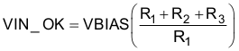
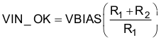
The VIN_OK setting is given by Equation 2.
The sum of the resistors is recommended to be no greater than 13 MΩ, that is, RSUM = R1 + R2 + R3 = 13 MΩ. Due to the sampling operation of the output resistors, lowering RSUM only increases quiescent current slightly as can be seen in Figure 22. Higher resistors may result in poor output voltage regulation and/or input voltage power-good threshold accuracies due to noise pickup through the high-impedance pins or reduction of effective resistance due to parasitic resistance created from board assembly residue. See Layout for more details.
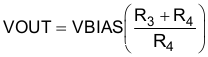
If it is preferred to separate the VOUT and VIN_OK resistor strings, two separate strings of resistors could be used as shown in Figure 62. The OUT DC set point is then given by Equation 3.
The VIN_OK setting is then given by Equation 4.
If it is preferred to disable the VIN_OK setting, the VIN_OK_SET pin can be tied to VIN. To set VOUT in this configuration, use Equation 3. To tighten the DC set point accuracy, use external resistors with better than 1% resistor tolerance. Because output voltage ripple has a large effect on input line regulation and the output load regulation, using a larger output capacitor will improve both line and load regulation.
9.3.3 Nano-Power Management and Efficiency
The high efficiency of the TPS6273x is achieved through the proprietary Nano-Power management circuitry and algorithm. This feature essentially samples and holds all references in order to reduce the average quiescent current. That is, the internal circuitry is only active for a short period of time and then off for the remaining period of time at the lowest feasible duty cycle. A portion of this feature can be observed in Figure 66 where the VRDIV node is monitored. Here, the VRDIV node provides a connection to the input (larger voltage level) and generates the output reference (lower-voltage level) for a short period of time. The divided down value of input voltage is compared to VBIAS and the output voltage reference is sampled and held to get the VOUT_SET point. Because this biases a resistor string, the current through these resistors is only active when the Nano-Power management circuitry makes the connection — hence, reducing the overall quiescent current due to the resistors. This process repeats every 64 ms. Similarly, the VIN_OK level is monitored every 64 ms, as shown in Figure 55.
The efficiency versus output current and efficiency versus input voltage are plotted for three different output voltages for both the TPS62736 and TPS62737 devices in Typical Characteristics. All data points were captured by averaging the overall input current. This must be done, due to the periodic biasing scheme implemented through the Nano-Power management circuitry. The input current efficiency data was gathered using a source meter set to average over at least 25 samples and at the highest accuracy sampling rate. Each data point takes a long period of time to gather in order to properly measure the resulting input current when calculating the efficiency.
9.4 Device Functional Modes
9.4.1 Enable Controls
There are two enable pins implemented in the TPS6273x in order to maximize the flexibility of control for the system. The EN1 pin is considered to be the chip enable. If EN1 is set to a 1 then the entire chip is placed into ship mode. If EN1 is 0 then the chip is enabled. EN2 enables and disables the switching of the buck converter. When EN2 is low, the internal circuitry remains ON and the VIN_OK indicator still functions. This can be used to disable down-stream electronics in case of a low input-supply condition. When EN2 is 1, the buck converter operates normally.
Table 3. Enable Functionality Table
| EN1 PIN | EN2 PIN | FUNCTIONAL STATE |
|---|---|---|
| 0 | 0 | Partial standby mode. Buck switching converter is off, but VIN_OK indication is on |
| 0 | 1 | Buck mode and VIN_OK enabled |
| 1 | x | Full standby mode. Switching converter and VIN_OK indication is off (ship mode) |
9.4.2 Startup Behavior
The TPS6273x has two startup responses: 1) from the ship-mode state (EN1 transitions from high to low), and 2) from the standby state (EN2 transitions from low to high). The first startup response out of the ship-mode state has the longest time duration due to the internal circuitry being disabled. This response is shown in Figure 70 for the TPS62736 and Figure 60 for the TPS62737. The startup time takes approximately 100 ms due to the internal Nano-Power management circuitry needing to complete the 64 ms sample and hold cycle.
Startup from the standby state is shown in Figure 71 for the TPS62736 and Figure 61 for the TPS62737. This response is much faster due to the internal circuitry being pre-enabled. The startup time from this state is entirely dependent on the size of the output capacitor. The larger the capacitor, the longer it will take to charge during startup. The TPS6273x can startup into a prebiased output voltage.