SLVSBO4C October 2012 – December 2014 TPS62736 , TPS62737
UNLESS OTHERWISE NOTED, this document contains PRODUCTION DATA.
- 1 Features
- 2 Applications
- 3 Description
- 4 Revision History
- 5 Description (continued)
- 6 Device Voltage Options
- 7 Pin Configuration and Functions
- 8 Specifications
- 9 Detailed Description
- 10Application and Implementation
- 11Power Supply Recommendations
- 12Layout
- 13Device and Documentation Support
- 14Mechanical, Packaging, and Orderable Information
1 Features
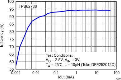
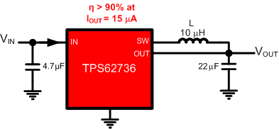
- Industry's Highest Efficiency at Low Output Currents: > 90% With IOUT = 15 µA
-
Ultra-Low Power Buck Converter
- TPS62736 Optimized for 50-mA Output Current
- TPS62737 Optimized for 200-mA Output Current
- 1.3-V to 5-V Resistor Programmable Output Voltage Range
- 2-V to 5.5-V Input Operating Range
- 380-nA and 375-nA Quiescent Current During Active Operation for TPS62736 and TPS62737
- 10-nA Quiescent Current During Ship Mode Operation
- 2% Voltage Regulation Accuracy
- 100% Duty Cycle (Pass Mode)
- EN1 and EN2 Control
- Two Power-Off States:
- Shipmode (Full Power-Off State)
- Standby Mode Includes VIN_OK Indication
- Two Power-Off States:
- Input Power-Good Indication (VIN_OK)
- Push-Pull Driver
- Resistor Programmable Threshold Level
2 Applications
- Ultra-Low Power Applications
- 2-Cell and 3-Cell Alkaline-Powered Applications
- Energy Harvesting
- Solar Chargers
- Thermal Electric Generator (TEG) Harvesting
- Wireless Sensor Networks (WSN)
- Low-Power Wireless Monitoring
- Environmental Monitoring
- Bridge and Structural Health Monitoring (SHM)
- Smart Building Controls
- Portable and Wearable Health Devices
- Entertainment System Remote Controls
3 Description
The TPS6273x family provides a highly integrated ultra low power buck converter solution that is well suited for meeting the special needs of ultra-low power applications such as energy harvesting. The TPS6273x provides the system with an externally programmable regulated supply to preserve the overall efficiency of the power-management stage compared to a linear step-down converter. This regulator is intended to step-down the voltage from an energy storage element such as a battery or super capacitor to supply the rail to low-voltage electronics. The regulated output has been optimized to provide high efficiency across low-output currents (<10 µA) to high currents (200 mA).
The TPS6273x integrates an optimized hysteretic controller for low-power applications. The internal circuitry uses a time-based sampling system to reduce the average quiescent current.
Device Information(1)
| PART NUMBER | PACKAGE | BODY SIZE (NOM) |
|---|---|---|
| TPS6273x | VQFN (14) | 3.50 mm × 3.50 mm |
- For all available packages, see the orderable addendum at the end of the datasheet.
Efficiency vs Output Current