SLVSC52B July 2013 – September 2015 TPS62152-Q1
PRODUCTION DATA.
- 1 Features
- 2 Applications
- 3 Description
- 4 Revision History
- 5 Pin Configuration and Functions
- 6 Specifications
-
7 Detailed Description
- 7.1 Overview
- 7.2 Functional Block Diagram
- 7.3
Feature Description
- 7.3.1 Pulse-Width Modulation (PWM) Operation
- 7.3.2 100% Duty-Cycle Operation
- 7.3.3 Enable / Shutdown (EN)
- 7.3.4 Soft Start or Tracking (SS/TR)
- 7.3.5 Current-Limit and Short-Circuit Protection
- 7.3.6 Power Good (PG)
- 7.3.7 Pin-Selectable Output Voltage (DEF)
- 7.3.8 Frequency Selection (FSW)
- 7.3.9 Undervoltage Lockout (UVLO)
- 7.3.10 Thermal Shutdown
- 7.3.11 Tracking Function
- 7.3.12 Feedback Pin (FB)
- 7.4 Device Functional Modes
- 8 Application and Implementation
- 9 Power Supply Recommendations
- 10Layout
- 11Device and Documentation Support
- 12Mechanical, Packaging, and Orderable Information
1 Features
- Qualified for Automotive Applications
- AEC-Q100 Qualified With the Following Results:
- DCS-Control Topology
- Input Voltage Range: 4 V to 17 V
- Up to 1-A Output Current
- Fixed Output Voltage: 3.3 V
- Programmable Soft Start and Tracking
- Seamless Power-Save Mode Transition
- Quiescent Current of 17 µA (Typ.)
- Selectable Operating Frequency
- Power-Good Output
- 100% Duty-Cycle Mode
- Short-Circuit Protection
- Overtemperature Protection
- Available in a 3-mm × 3-mm, VQFN-16 Package
2 Applications
- Automotive Infotainment and Cluster
- Instrument Cluster
- Center Stack
- Head Unit
- Rear-Seat Entertainment
- Advanced Driver-Assistance System (ADAS)
- Surround View
- Rear-View Camera
- Front Camera
3 Description
The TPS62152-Q1 device is an easy-to-use
synchronous step-down dc-dc converter optimized for applications with high power density and features a fixed 3.3-V output with a current capability of up to
1 A. A high switching frequency of 2.5 MHz (typical) allows the use of small inductors and provides fast transient response as well as high output-voltage accuracy by use of the DCS-Control topology.
With a wide operating input voltage range of 4 V to 17 V, the device is ideally suited for systems powered from either a Li-Ion or other batteries as well as from 12-V intermediate power rails.
The soft-start pin controls the output voltage start-up ramp, which allows operation either as a standalone power supply or in tracking configurations. Power sequencing is also possible by configuring the enable and open-drain power-good pins.
In power-save mode, the device draws quiescent current of about 17 μA from VIN. Power-save mode, entered automatically and seamlessly if the load is small, maintains high efficiency over the entire load range. Entering shutdown mode turns the device off, and shutdown current consumption is less than 2 μA.
The device package is a 16-pin VQFN measuring
3-mm × 3-mm (RGT) and has an exposed thermal pad for better thermal performance.
Device Information(1)
| PART NUMBER | PACKAGE | BODY SIZE (NOM) |
|---|---|---|
| TPS62152-Q1 | VQFN (16) | 3.00 mm × 3.00 mm |
- For all available packages, see the orderable addendum at the end of the datasheet.
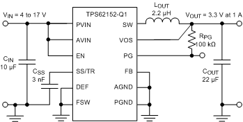
Typical Application

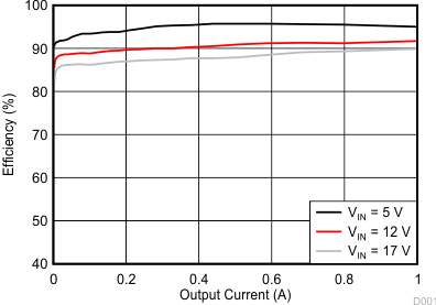
Efficiency Vs Output Current
