ZHCS174C January 2014 – October 2014 TPS61230 , TPS61232
UNLESS OTHERWISE NOTED, this document contains PRODUCTION DATA.
- 1 特性
- 2 应用范围
- 3 说明
- 4 修订历史记录
- 5 Device Comparison Table
- 6 Pin Configuration and Functions
- 7 Specifications
- 8 Detailed Description
-
9 Applications and Implementation
- 9.1 Application Information
- 9.2
Typical Applications
- 9.2.1 TPS61230 2.3-V to 5.5-V Input, 5-V Output Converter
- 9.2.2 TPS61230 2.3-V to 5.5-V Input, 3.5-V Output Converter
- 9.2.3 TPS61230 Application with Feed Forward Capacitor for Best Transient Response
- 10Power Supply Recommendations
- 11Layout
- 12器件和文档支持
- 13机械封装和可订购信息
8 Detailed Description
8.1 Overview
The TPS6123x synchronous step-up converter typically operates at a quasi-constant 2-MHz frequency pulse width modulation (PWM) at moderate to heavy load currents. At light load currents, the TPS6123x converter operates in power-save mode with pulse frequency modulation (PFM). The converter uses a novel quasi-constant on-time valley current mode control scheme which provides excellent transient line / load response with minimal output capacitance. Internal loop compensation simplifies the design process while minimizing the number of external components. The TPS6123x device can smoothly transit in and out of zero duty cycle mode (high side FET full on). Therefore the output can be kept as close as possible to its regulation limits even though the converter is subject to an input voltage that tends to be excessive.
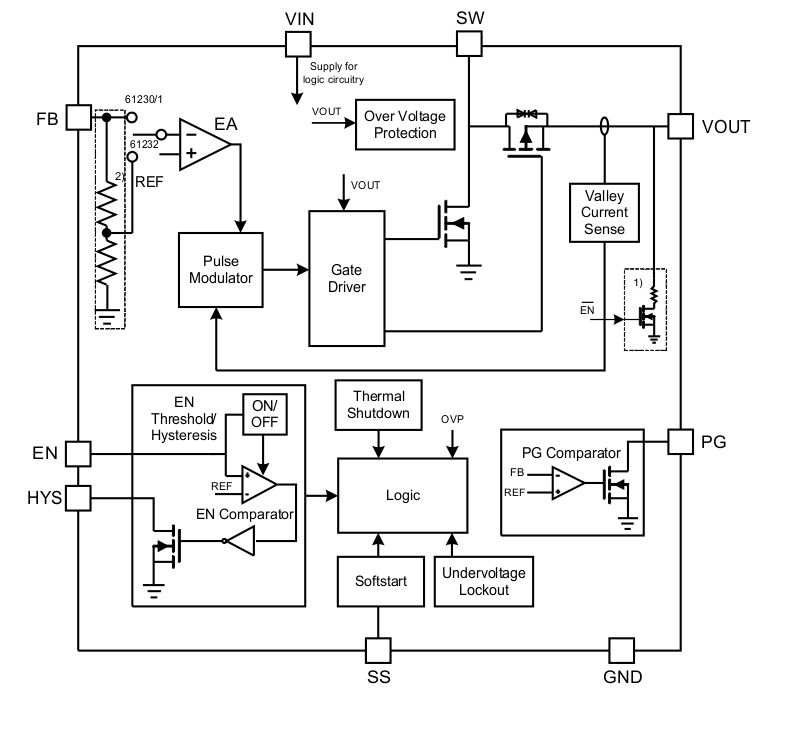
8.2 Functional Block Diagram
8.3 Feature Description
8.3.1 Startup
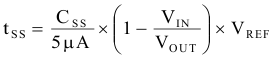
In boost mode (PWM or PFM), the rectifying switch is turned on first until the output capacitor is charged to 0.5 V with the current limit of 550 mA after the device is enabled. Then, the output capacitor is continuously charged to a value close to the input voltage. This is called the pre-charge phase. During the pre-charge phase, the output current is limited by the pre-charge current limit of the high side rectifying switch and the SS pin voltage follows the FB voltage (in the TPS61232, the SS pin follows the internal FB voltage). Once the output capacitor has been biased to the input voltage, the device starts switching. This is called the soft start phase. During the soft start phase, the SS pin voltage limits the FB pin voltage, and the output voltage rising slope follows the SS pin voltage slope. The capacitor connected to the SS pin is charged by the internal bias current of ISS, giving the time of the soft start phase shown in Equation 1. The larger the soft start capacitor, the longer the soft start phase time. Leaving the SS pin floating sets the minimum soft startup phase time. The device finishes the soft start phase and operates normally when the nominal output voltage is reached.
The SS pin voltage is discharged in the cases when the device gets disabled by the EN pin, thermal shutdown and undervoltage lockout. The SS pin may be left floating to disable the soft start phase and start up with the fastest time. In zero duty cycle mode, only the pre-charge phase works during startup.
8.3.2 Current Limit Operation
The device employs a valley current sensing scheme. Switch valley current limit detection occurs during the off time through sensing of the voltage drop across the synchronous rectifier. If the current is above the valley current limit level when it is time to turn off the synchronous rectifier, the device instead keeps the synchronous rectifier on until its current decreases below the valley current limit level. The maximum continuous output current IOUT(MAX), before entering switch valley current limit operation, is defined by Equation 2.
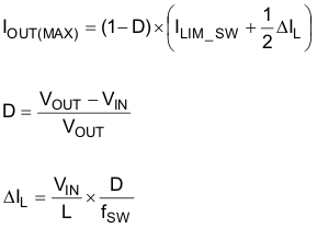
Where
ILIM_SW = Switch valley current limit
L = Inductor value
fSW = Switching frequency
When the switch current limit is reached, the output voltage decreases from further load increase. The switch valley current limit works in PWM, PFM and Zero Duty Cycle Mode operations.
Another current limit scheme, pre-charge current limit, ILIM_Pre is implemented. Pre-charge current limit detection works when VOUT < VOUT_NOM and VOUT < VIN . It can happen when the device is in the pre-charge phase or an over load condition. It impacts the minimum load resistance at startup as shown in Figure 14 and Figure 27.
8.3.3 Enable/Disable
The EN pin is connected to an ON/OFF detector (ON/OFF) and an input of the Enable Comparator, shown in the functional block diagram. With a voltage level of 0.4 V or less at the EN pin, the ON/OFF detector turns the device into Shutdown mode and the quiescent current is reduced to typically 1.5 uA. In this mode, the EN comparator and the entire internal control circuitry are switched off. A voltage level of typically 0.9 V at the EN pin triggers the ON/OFF detector and activates the internal reference, the EN comparator and the UVLO comparator. Once the ON/OFF detector has tripped, the quiescent current into the VIN pin is typically 1.5 μA.
The TPS6123x starts regulation once the voltage at the EN pin trips the threshold VEN_TH_ON and the VIN pin voltage is above the UVLO threshold. The device enters startup and ramps up the output voltage. The TPS6123x stops regulation once the voltage on the EN pin falls blow the threshold VEN_TH_OFF or the VIN pin voltage falls below the UVLO threshold. For proper operation, The EN pin must be terminated and must not be left floating. An external logic signal applied directly to the EN pin can enable/disable the device. The device can be driven into shutdown mode by pulling the EN pin to GND. In this mode, true load disconnect between the battery and load prevents current flow from VIN to VOUT, as well as reverse flow from VOUT to VIN.
8.3.4 Undervoltage Lockout
An under voltage lockout is implemented to avoid mis-operation of the device at low input voltages. It shuts down the device with voltages lower than VUVLO.
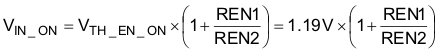
Use the HYS pin to configure a new undervoltage lockout threshold and hysteresis shown in Figure 10 and Equation 3. The new thresholds must be higher than VUVLO; otherwise it does not work. The devices holds the HYS pin low until the EN voltage rises above VEN_TH_ON. Then, the HYS pin goes high impedance.
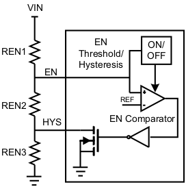 Figure 10. EN Comparator threshold and hysteresis setting

8.3.5 Output Capacitor Discharge, TPS61231
To make sure the device starts up under defined conditions, the output capacitor of the TPS61231 gets discharged by the VOUT pin with a typical discharge resistor of RDIS in the cases when the device gets disabled by the EN pin, thermal shutdown, and undervoltage lockout.
8.3.6 Power Good Output
The PG output is low when the output voltage is below 90% of its nominal value. The PG pin becomes high impedance once the output is higher than 95% of its nominal voltage. The PG pin is an open drain output and is specified to sink up to 500 µA. This PG output requires a pull-up resistor that cannot be connected to any voltage higher than 5.5 V. PG is held low when the device is disabled by the EN pin and thermal shutdown.
8.3.7 Over Voltage Protection
The device stops switching as soon as the output voltage exceeds VOVP. When the output voltage falls 0.15V below the OVP threshold, the device resumes normal operation until the output voltage exceeds the OVP threshold again.
8.3.8 Thermal Shutdown
The device goes into thermal shutdown and stops switching once the junction temperature exceeds TJSD. Once the junction temperature falls below the threshold, it returns to normal operation automatically.
8.4 Device Functional Modes
The TPS6123x boost converter family has three operation modes, as shown in Table 1.
Table 1. Operation Mode Description
| MODE | DESCRIPTION | CONDITION |
|---|---|---|
| PWM | Boost in normal switching operation | VIN < VOUT + 0.2 V, heavy load |
| PFM | Boost in power save operation | VIN < VOUT + 0.2 V, light load |
| Zero Duty Cycle | Zero duty cycle operation | VOUT < VIN ≤ VOUT + 0.24 V and VOUT ≥ VOUT_NOM |
8.4.1 Boost Normal Mode
The TPS6123x boost converter family typically operates at a quasi-constant 2-MHz frequency pulse width modulation (PWM) at moderate to heavy load currents. Based on the VIN/VOUT ratio, a simple circuit predicts the required on-time. At the beginning of the switching cycle, the low-side N-MOS switch, shown in the functional block diagram, is turned on and the inductor current ramps up to a peak current that is defined by the on-time and the inductance. In the second phase, once this peak current is reached, the current comparator trips, the on-timer is reset turning off the low-side N-MOS switch and turning on the high-side rectifying switch. The current through the inductor then decays to an internally set valley current. Once this occurs, the on-timer is set to turn the boost switch back on again and the cycle is repeated.
8.4.2 Boost Power Save Mode
The device integrates a power save mode with pulse frequency modulation (PFM) to improve efficiency at light load. In power save mode, the device only switches when the output voltage trips below a set threshold voltage. It ramps up the output with several pulses and enters the power save mode when the output voltage exceeds the set threshold voltage. PFM is left and PWM mode entered when the inductor current becomes discontinuous. The DC output voltage in PFM mode rises above the nominal output voltage in PWM mode by 0.7%.
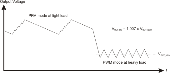 Figure 11. Output Voltage in PFM/PWM Mode
8.4.3 Zero Duty Cycle Mode
When the input voltage is lower than VOUT + 0.24 V and VOUT is higher than the nominal output voltage, the device automatically changes to a Zero Duty Cycle Mode. In Zero Duty Cycle Mode, the rectifying switch is constantly turned on and the low side switch is turned off. The output voltage in this mode depends on the resistance between the input and the output, calculated as: