ZHCS174C January 2014 – October 2014 TPS61230 , TPS61232
UNLESS OTHERWISE NOTED, this document contains PRODUCTION DATA.
- 1 特性
- 2 应用范围
- 3 说明
- 4 修订历史记录
- 5 Device Comparison Table
- 6 Pin Configuration and Functions
- 7 Specifications
- 8 Detailed Description
-
9 Applications and Implementation
- 9.1 Application Information
- 9.2
Typical Applications
- 9.2.1 TPS61230 2.3-V to 5.5-V Input, 5-V Output Converter
- 9.2.2 TPS61230 2.3-V to 5.5-V Input, 3.5-V Output Converter
- 9.2.3 TPS61230 Application with Feed Forward Capacitor for Best Transient Response
- 10Power Supply Recommendations
- 11Layout
- 12器件和文档支持
- 13机械封装和可订购信息
6 Pin Configuration and Functions
11-PIN VSON
DRC PACKAGE
(Top View)
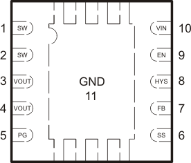
Pin Functions
| PIN | I/O | DESCRIPTION | |
|---|---|---|---|
| NAME | NUMBER | ||
| SW | 1,2 | PWR | The switch pin of the converter. It is connected to the drain of the internal Power MOSFETs. |
| VOUT | 3,4 | PWR | Boost converter output pin. |
| PG | 5 | OUT | Power Good open drain output. Can be left floating if not used. |
| SS | 6 | IN | Soft startup pin. A soft startup capacitor connects to this pin to set the soft start time. |
| FB | 7 | IN | Voltage feedback of adjustable versions. Must be connected to VOUT on fixed output voltage version. |
| HYS | 8 | OUT | EN hysteresis program pin. See the application section for details. Can be left floating if not used. |
| EN | 9 | IN | Enable logic input. Logic HIGH enables the device. Logic LOW disables the device and turns it into shutdown mode. This pin must be terminated. |
| VIN | 10 | IN | Supply voltage pin. |
| GND | 11 | PWR | Ground pin. |