SLVS776B January 2009 – November 2014 TPS61220 , TPS61221 , TPS61222
PRODUCTION DATA.
- 1 Features
- 2 Applications
- 3 Description
- 4 Simplified Schematic
- 5 Revision History
- 6 Pin Configuration and Functions
- 7 Specifications
- 8 Parameter Measurement Information
- 9 Detailed Description
- 10Applications and Implementation
- 11Power Supply Recommendations
- 12Layout
- 13Device and Documentation Support
- 14Mechanical, Packaging, and Orderable Information
10 Applications and Implementation
NOTE
Information in the following applications sections is not part of the TI component specification, and TI does not warrant its accuracy or completeness. TI’s customers are responsible for determining suitability of components for their purposes. Customers should validate and test their design implementation to confirm system functionality.
10.1 Application Information
The TPS6122x family devices provide a power-supply solution for products powered by either a single-cell, two-cell, or three-cell alkaline, NiCd or NiMH, or one-cell Li-Ion or Li-polymer battery. Use the following design procedure to select component values for the TPS61220 device and the TPS61222 device. Alternatively, use the SwitcherPro™ tool. This section presents a simplified discussion of the design process.
10.2 Typical Applications
10.2.1 Specific Application, Fixed Output Voltage Supply
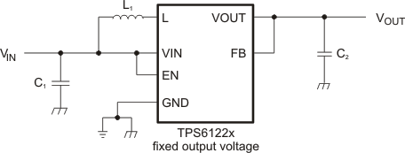 Figure 26. Typical Application Circuit For Fixed Output Voltage Option
10.2.1.1 Design Requirements
- Single 5 V output at up to 60 mA
- Power source, two AA alkaline cells
- Greater than 90% conversion efficiency
10.2.1.2 Detailed Design Procedure
10.2.1.2.1 Device Choice
The TPS61222 DC/DC converter is intended for systems powered by anything from a single cell through up to three Alkaline, NiCd or NiMH cells with a total typical pin voltage between 0.7 V and 5.5 V. They can also be used in systems powered by one-cell Li-Ion or Li-Polymer batteries with a typical voltage between 2.5 V and 4.2 V. Additionally, any other voltage source with a typical output voltage between 0.7 V and 5.5 V can be used with the TPS61222.
10.2.1.2.2 Programming The Output Voltage
In the fixed-voltage version used for this example, the output voltage is set by an internal resistor divider. The FB pin is used to sense the output voltage. To configure the device properly, connect the FB pin directly to VOUT as shown in Figure 26.
10.2.1.2.3 Inductor Selection
To make sure that the device can operate, a suitable inductor must be connected between pin VIN and pin L. Inductor values of 4.7 μH show good performance over the whole input and output voltage range.
Choosing other inductance values affects the switching frequency f proportional to 1/L as shown in Equation 1.
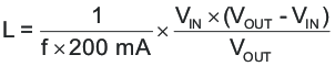
Choosing inductor values higher than 4.7 μH can improve efficiency due to reduced switching frequency and therefore with reduced switching losses. Using inductor values below 2.2 μH is not recommended.
Having selected an inductance value, the peak current for the inductor in steady-state operation can be calculated. Equation 2 gives the peak-current estimate.
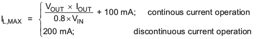
Equation 2 provides a suitable inductor current rating. However, remember that load transients and error conditions may cause higher inductor currents.
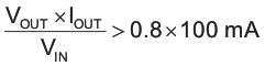
Equation 3 provides an easy way to estimate whether the device will work in continuous or discontinuous operation depending on the operating points. As long as the Equation 3 is true, continuous operation is typically established. If Equation 3 becomes false, discontinous operation is typically established.
The following inductor series from different suppliers have been used with TPS6122x converters:
Table 2. List Of Inductors
| VENDOR | INDUCTOR SERIES |
|---|---|
| Coilcraft | EPL3015 |
| EPL2010 | |
| Murata | LQH3NP |
| Tajo Yuden | NR3015 |
| Wurth Elektronik | WE-TPC Typ S |
10.2.1.2.4 Capacitor Selection
10.2.1.2.4.1 Input Capacitor
An input capacitor value of at least 10 μF is recommended to improve transient behavior of the regulator and EMI behavior of the total power supply circuit. A ceramic capacitor placed as close as possible to the VIN and GND pins of the IC is recommended.
10.2.1.2.4.2 Output Capacitor
For the output capacitor C2, small ceramic capacitors are recommended, placed as close as possible to the VOUT and GND pins of the IC. If, for any reason, the application requires the use of large capacitors which cannot be placed close to the IC, the use of a small ceramic capacitor with a capacitance value of around 2.2μF in parallel to the large one is recommended. This small capacitor should be placed as close as possible to the VOUT and GND pins of the IC.
A minimum capacitance value of 4.7 μF should be used, 10 μF is recommended. If the inductor value exceeds 4.7 μH, the value of the output capacitance value needs to be half the inductance value or higher for stability reasons, see Equation 4.

The TPS6122x is not sensitive to the ESR in terms of stability. However, low ESR capacitors, such as ceramic capacitors, are recommended anyway to minimize output voltage ripple. If heavy load changes are expected, increase the output capacitor value to avoid output voltage drops during fast load transients.
10.2.1.3 Application Curves
Figure 27 shows the excellent efficiency of the converter, which remains above 80% even with heavily discharged cells.
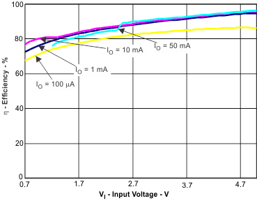 Figure 27. TPS61222 Performance
10.2.2 Specific Application, Variable Output Voltage Supply
 Figure 28. Application Circuit For Adjustable Output Voltage Option
10.2.2.1 Design Requirements
- Single 4.2 V output at up to 50 mA
- Power source, two AA alkaline cells
- Greater than 80% conversion efficiency
10.2.2.2 Detailed Design Procedure
The design procedure for this application is identical to that for the fixed-output supply except for programming the output voltage.
10.2.2.2.1 Device Selection
This application example uses the TPS61220 so that the output voltage can be set at 4.2 V.
10.2.2.2.2 Programming The Output Voltage
In the adjustable output versions, an external resistor divider is used to adjust the output voltage. The resistor divider must be connected between VOUT, FB and GND as shown in Figure 28. When the output voltage is regulated properly, the typical voltage value at the FB pin is 500 mV for the adjustable devices. The maximum recommended value for the output voltage is 6.0 V. The current through the resistor divider should be about 100 times greater than the current into the FB pin. The typical current into the FB pin is 0.01 μA, and the voltage across the resistor between FB and GND, R2, is typically 500 mV. Based on those two values, the recommended value for R2 should be lower than 500 kΩ, in order to set the divider current to 1 μA or higher. The value of the resistor connected between VOUT and FB, R1, depending on the needed output voltage (VOUT), can be calculated using Equation 5:
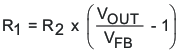
For this example, if an output voltage of 4.2 V is needed, a 1.2-MΩ resistor is calculated for R1 when 160 kΩ is selected for R2. This would yield an output voltage of 4.25 V, neglecting resistor tolerances.
10.2.2.2.3 Inductor Selection
See Inductor Selection for a discussion on inductor choice.
10.2.2.2.4 Capacitor Selection
The procedure for selecting capacitors is the same as for the fixed output voltage circuit. See Capacitor Selection.
10.2.2.3 Application Curves
Figure 29 shows the excellent efficiency of the converter, which remains above 80% with heavily discharged cells.
Figure 29. TPS61220 Performance