SLUS851D October 2008 – October 2014 TPS54231
PRODUCTION DATA.
- 1 Features
- 2 Applications
- 3 Description
- 4 Simplified Schematic
- 5 Revision History
- 6 Pin Configuration and Functions
- 7 Specifications
-
8 Detailed Description
- 8.1 Overview
- 8.2 Functional Block Diagram
- 8.3
Feature Description
- 8.3.1 Fixed-Frequency PWM Control
- 8.3.2 Voltage Reference (Vref)
- 8.3.3 Bootstrap Voltage (BOOT)
- 8.3.4 Enable and Adjustable Input Undervoltage Lockout (VIN UVLO)
- 8.3.5 Programmable Slow Start Using SS Pin
- 8.3.6 Error Amplifier
- 8.3.7 Slope Compensation
- 8.3.8 Current-Mode Compensation Design
- 8.3.9 Overcurrent Protection and Frequency Shift
- 8.3.10 Overvoltage Transient Protection
- 8.3.11 Thermal Shutdown
- 8.4 Device Functional Modes
-
9 Application and Implementation
- 9.1 Application Information
- 9.2
Typical Application
- 9.2.1 Design Requirements
- 9.2.2 Detailed Design Procedure
- 9.2.3 Application Curves
- 10Power Supply Recommendations
- 11Layout
- 12Device and Documentation Support
- 13Mechanical, Packaging, and Orderable Information
9 Application and Implementation
NOTE
Information in the following applications sections is not part of the TI component specification, and TI does not warrant its accuracy or completeness. TI’s customers are responsible for determining suitability of components for their purposes. Customers should validate and test their design implementation to confirm system functionality.
9.1 Application Information
The TPS54231 device is typically used as a step-down converter, which converts a voltage from 3.5 V to 28 V to a lower voltage. WEBENCH software is available to aid in the design and analysis of circuits.
For additional design needs, see the following devices:
| PARAMETER | TPS54231 | TPS54232 | TPS54233 | TPS54331 | TPS54332 |
|---|---|---|---|---|---|
| IO(max) | 2 A | 2 A | 2 A | 3 A | 3.5 A |
| Input voltage range | 3.5 to 28 V | 3.5 to 28 V | 3.5 to 28 V | 3.5 to 28 V | 3.5 to 28 V |
| Switching frequency (typ) | 570 kHz | 1000 kHz | 285 kHz | 570 kHz | 1000 kHz |
| Switch current limit (min) | 2.3 A | 2.3 A | 2.3 A | 3.5 A | 4.2 A |
| Pin and Package | 8SOIC | 8SOIC | 8SOIC | 8SOIC | 8SO PowerPAD™ |
9.2 Typical Application
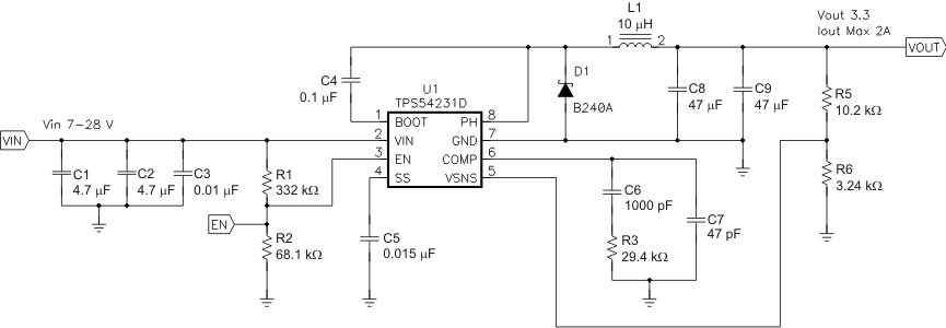 Figure 10. Typical Application Schematic
9.2.1 Design Requirements
For this design example, use the parameters listed in Table 3 as the input parameters.
Table 3. Design Parameters
| DESIGN PARAMETER | EXAMPLE VALUE |
|---|---|
| Input voltage range | 7 to 28 V |
| Output voltage | 3.3 V |
| Input ripple voltage | 300 mV |
| Output ripple voltage | 30 mV |
| Output current rating | 2 A |
| Operating Frequency | 570 kHz |
9.2.2 Detailed Design Procedure
The following design procedure can be used to select component values for the TPS54231 device. Alternately, the WEBENCH Software can be used to generate a complete design. The WEBENCH Software uses an iterative design procedure and accesses a comprehensive database of components when generating a design. This section presents a simplified discussion of the design process.
9.2.2.1 Switching Frequency
The switching frequency for the TPS54231 device is fixed at 570 kHz.
9.2.2.2 Output Voltage Set Point
The output voltage of the TPS54231 device is externally adjustable using a resistor divider network. As shown in Figure 10, this divider network is comprised of R5 and R6. The relationship of the output voltage to the resistor divider is given by Equation 4 and Equation 5.
Select a value of R5 to be approximately 10 kΩ. Slightly increasing or decreasing the value of R5 can result in closer output-voltage matching when using standard value resistors. In this design, R4 = 10.2 kΩ and R = 3.24 kΩ, resulting in a 3.31-V output voltage. The 0-Ω resistor R4 is provided as a convenient location to break the control loop for stability testing.
9.2.2.3 Input Capacitors
The TPS54231 device requires an input decoupling capacitor and, depending on the application, a bulk input capacitor. The typical recommended value for the decoupling capacitor is 10 μF. A high-quality ceramic type X5R or X7R is recommended. The voltage rating should be greater than the maximum input voltage. A smaller value can be used as long as all other requirements are met; however a value of 10 μF has been shown to work well in a wide variety of circuits. Additionally, some bulk capacitance may be required, especially if the TPS54231 device circuit is not located within about 2 inches from the input voltage source. The value for this capacitor is not critical but should be rated to handle the maximum input voltage including ripple voltage, and should filter the output so that input ripple voltage is acceptable. For this design two 4.7-μF capacitors are used for the input decoupling capacitor. The capacitors are X7R dielectric rated for 50 V. The equivalent series resistance (ESR) is approximately 2 mΩ, and the current rating is 3 A. Additionally, a small 0.01-μF capacitor is included for high frequency filtering.
Use Equation 6 to calculate the input ripple voltage.
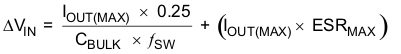
where
- IOUT(MAX) is the maximum load current
- ƒSW is the switching frequency
- CBULK is the bulk capacitor value
- ESRMAX is the maximum series resistance of the bulk capacitor
The maximum RMS ripple current must also be checked. For worst case conditions, use Equation 7 to calculate the maximum-RMS input ripple current, ICIN(RMS).
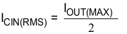
In this case, the input ripple voltage is 113 mV and the RMS ripple current is 1 A.
NOTE
The actual input voltage ripple is greatly affected by parasitics associated with the layout and the output impedance of the voltage source.
The actual input voltage ripple for this circuit is listed in Table 3 and is larger than the calculated value. This measured value is still below the specified input limit of 300 mV. The maximum voltage across the input capacitors would be VIN(MAX) plus ΔVIN / 2. The selected bulk and bypass capacitors are each rated for 50 V and the ripple current capacity is greater than 3 A, both providing ample margin. The maximum ratings for voltage and current must not be exceeded under any circumstance.
9.2.2.4 Output Filter Components
Two components need to be selected for the output filter, L1 and C2. Because the TPS54231 device is an externally compensated device, a wide range of filter component types and values can be supported.
9.2.2.4.1 Inductor Selection
To calculate the minimum value of the output inductor, use Equation 8.
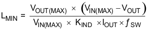
where
- KIND is a coefficient that represents the amount of inductor ripple current relative to the maximum output current
In general, this value is at the discretion of the designer; however, the following guidelines may be used. For designs using low-ESR output capacitors such as ceramics, a value as high as KIND = 0.3 may be used. When using higher ESR output capacitors, KIND = 0.2 yields better results.
For this design example, use KIND = 0.3 and the minimum inductor value is calculated as 8.5 μH. For this design, a large value was selected: 10 μH.
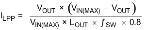
For the output filter inductor, do not exceed the RMS current and saturation current ratings. Use Equation 9 to calculate the inductor ripple current (ILPP).
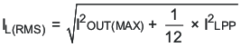
Use Equation 10 to calculate the RMS inductor current.
Use Equation 11 to calculate the peak inductor current.
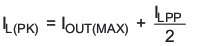
For this design, the RMS inductor current is 2.008 A and the peak inductor current is 2.32 A. The selected inductor is a Coilcraft MSS1038-103NL, 10 μH. This inductor has a saturation current rating of 3.04 A and an RMS current rating of 2.90 A, which meets these requirements. Smaller or larger inductor values can be used depending on the amount of ripple current the designer wants to allow so long as the other design requirements are met. Larger value inductors will have lower AC current and result in lower output voltage ripple, while smaller inductor values will increase AC current and output voltage ripple. In general, inductor values for use with the TPS54231 device are in the range of 6.8 μH to 47μH.
9.2.2.4.2 Capacitor Selection
The important design factors for the output capacitor are DC voltage rating, ripple current rating, and equivalent series resistance (ESR). The DC voltage and ripple current ratings cannot be exceeded. The ESR is important because along with the inductor current it determines the amount of output ripple voltage. The actual value of the output capacitor is not critical, but some practical limits do exist. Consider the relationship between the desired closed-loop crossover frequency of the design and LC corner frequency of the output filter. In general, keeping the closed-loop crossover frequency at less than 1/5 of the switching frequency is desired. With high switching frequencies such as the 570-kHz frequency of this design, internal circuit limitations of the TPS54231 device limit the practical maximum crossover frequency to about 25 kHz. In general, the closed-loop crossover frequency should be higher than the corner frequency determined by the load impedance and the output capacitor. Use Equation 12 to calculate the limits of the minimum capacitor value for the output filter.
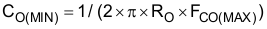
where
- RO is the output load impedance (VO / IO)
- FCO(MAX) is the desired crossover frequency
For a desired maximum crossover of 25 kHz the minimum value for the output capacitor is approximately 3.6 μF. This value may not satisfy the output ripple voltage requirement. Use Equation 13 to estimate the output ripple voltage.
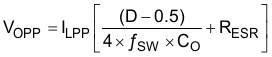
where
- D = Duty cycle (VOUT / VIN)
- CO = Output Capacitance
- RESR = Equivalent series resistance of the output capacitors
The peak-to-peak output voltage ripple consists of two terms. The first term is because of the AC ripple current (ILPP) charging and discharging the output capacitance in each switching cycle and the second term is because of the AC ripple current in the ESR of the output capacitor. These two terms could be out of phase and may add or subtract depending on the duty cycle. The required capacitance and ESR of the output filter capacitor must be selected to meet the allowable output ripple voltage requirement as specified in the initial design parameters.
Use Equation 14 to calculate the maximum RMS ripple current in the output capacitor.
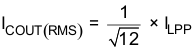
For this design example, two 47-μF ceramic output capacitors are selected for C8 and C9. These capacitors are TDK C3216X5R0J476M, rated at 6.3 V with a maximum ESR of 2 mΩ and a ripple current rating in excess of
3 A. The calculated total RMS ripple current is 184 mA (92 mA each) and the maximum total ESR required is 56 mΩ. These output capacitors exceed the requirements by a wide margin and result in a reliable, high-performance design.
NOTE
The actual capacitance in circuit may be less than the catalog value when the output is operating at the desired output of 3.3 V.
The selected output capacitor must be rated for a voltage greater than the desired output voltage plus half of the ripple voltage. Any derating amount must also be included. Other capacitor types work well with the TPS54231 device, depending on the needs of the application.
9.2.2.5 Compensation Components
The external compensation used with the TPS54231 device allows for a wide range of output filter configurations. A large range of capacitor values and types of dielectric are supported. The design example uses ceramic X5R dielectric output capacitors, but other types are supported.
A Type II compensation scheme is recommended for the TPS54231 device. The compensation components are selected to set the desired closed-loop crossover frequency and phase margin for output filter components. The Type II compensation has the following characteristics: a DC gain component, a low frequency pole, and a mid frequency zero-pole pair. The required compensation components are a resistor, RZ, in series with a capacitor, RZ, from the COMP pin to ground and a capacitor, CP, in parallel with RZ and CZ from the COMP pin to ground.
Use Equation 15 to calculate the DC gain.
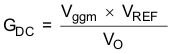
where
- Vggm = 800
- VREF = 0.8 V
Use Equation 16 to calculate the low-frequency pole.

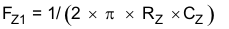
Use Equation 17 to calculate the mid-frequency zero.
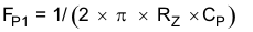
Use Equation 18 to calculate the mid-frequency pole.
The first step is to select the closed-loop crossover frequency. In general, the closed-loop crossover frequency should be less than 1/8 of the minimum operating frequency. However, for the TPS54231 device, not exceeding 25 kHz for the maximum closed-loop crossover frequency is recommended. The second step is to calculate the required gain and phase boost of the crossover network. By definition, the gain of the compensation network must be the inverse of the gain of the modulator and output filter. For this design example, where the ESR zero is much higher than the closed-loop crossover frequency, the gain of the modulator and output filter can be approximated by Equation 19:

where
- RSENSE = 1 Ω / 9
- FCO = Closed-loop crossover frequency
- CO = Output capacitance
Use Equation 20 to calculate the phase loss.

where
- RESR = Equivalent series resistance of the output capacitor
- RO = VO / IO
Now that the phase loss is known, the required amount of phase boost to meet the phase margin requirement can be determined. Use Equation 21 to calculate the required phase boost.

where
- PM = the desired phase margin
- PL = the phase loss calculated in Equation 20
A zero-pole pair of the compensation network will be placed symmetrically around the intended closed-loop frequency to provide maximum phase boost at the crossover point. The amount of separation can be determined by Equation 22. Use Equation 23 and Equation 24 to calculate the resultant zero and pole frequencies.

The low-frequency pole is set so that the gain at the crossover frequency is equal to the inverse of the gain of the modulator and output filter. Because of the relationships of the pole and zero frequencies, use Equation 25 to calculate the value of RZ.
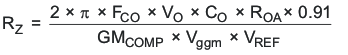
where
- VO = Output voltage
- CO = Output capacitance
- FCO = Desired crossover frequency
- ROA = 8.696 MΩ
- GMCOMP = 9 A/V
- Vggm = 800
- VREF = 0.8 V
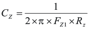
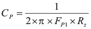
With the value of RZ known, use Equation 26 and Equation 27 to calculate the values of CZ and CP.
For this design, the two 47-μF output capacitors are used. For ceramic capacitors, the actual output capacitance is less than the rated value when the capacitors have a DC bias voltage applied which occurs in a DC-DC converter. The actual output capacitance may be as low as 41 μF. The combined ESR is approximately 0.002 Ω.
The desired crossover frequency is 25 kHz.
Using Equation 19 and Equation 20, the output stage gain and phase loss are equivalent as:
Gain = 5.9 dB
PL = –93.8 degrees
For 60 degrees of phase margin, Equation 21 requires 63.9 degrees of phase boost.
Use Equation 22, Equation 23, and Equation 24 to calculate the zero and pole frequencies of the following values:
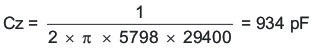
FZ1 = 5798 Hz
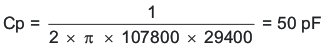
FP1 = 107.8 kHz
Use Equation 25 to calculate the value of RZ.

With the value of RZ set to the standard value of 29.4 kΩ, the values of Cz and CP can be calculated using Equation 26 and Equation 27.
Referring to Figure 10 and using standard values for R3, C6, and C7, the calculated values are as follows:
R3 = 29.4 kΩ
C6 = 1000 pF
C7 = 47 pF
Figure 16 shows the measured overall loop response for the circuit. The actual closed-loop crossover frequency is higher than intended at about 25 kHz which is primarily because of variation in the actual values of the output filter components and tolerance variation of the internal feed-forward gain circuitry. Overall, the design has greater than 60 degrees of phase margin and will be completely stable over all combinations of line and load variability.
9.2.2.6 Bootstrap Capacitor
Every TPS54231 design requires a bootstrap capacitor, C4. The bootstrap capacitor must be 0.1 μF. The bootstrap capacitor is located between the PH pin and BOOT pin. The bootstrap capacitor should be a high-quality ceramic type with X7R or X5R grade dielectric for temperature stability.
9.2.2.7 Catch Diode
The TPS54231 device is designed to operate using an external catch diode between the PH and GND pins. The selected diode must meet the absolute maximum ratings for the application. The Reverse voltage must be higher than the maximum voltage at the PH pin, which is VIN(MAX) + 0.5 V. The peak current must be greater than IOUT(MAX) plus on half the peak-to-peak inductor current. The forward-voltage drop should be small for higher efficiencies. The catch diode conduction time is (typically) longer than the high-side FET on time, so attention paid to diode parameters can make a marked improvement in overall efficiency. Additionally, check that the selected device is capable of dissipating the power losses. For this design, a Diodes, Inc. B240A is selected, with a reverse voltage of 40 V, forward current of 2 A, and a forward voltage drop of 0.5 V.
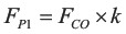
9.2.2.8 Output Voltage Limitations
Because of the internal design of the TPS54231 device, any given input voltage has both upper and lower output voltage limits. The upper limit of the output-voltage set point is constrained by the maximum duty cycle of 91% and is with Equation 31.

where
- VIN(MIN) = Minimum input voltage
- IO(MAX) = Maximum load current
- VD = Catch diode forward voltage
- RL = Output inductor series resistance
The equation assumes the maximum ON resistance for the internal high-side FET.
The lower limit is constrained by the minimum controllable on time which can be as high as 130 ns at 25°C junction temperature.
Use Equation 32 to calculate the approximate minimum output voltage for a given input voltage and minimum load current.

where
- VIN(MAX) = Maximum input voltage
- IO(MIN) = Minimum load current
- VD = Catch diode forward voltage
- RL = Output inductor series resistance
The normal ON resistance for the high-side FET in Equation 32 is assumed. Equation 32 accounts for worst case variation of operating-frequency set point. Any design operating near the operational limits of the device should be carefully checked to ensure proper functionality.
9.2.2.9 Power Dissipation Estimate
The following formulas show how to estimate the device power dissipation under continuous-conduction mode (CCM) operations. These formulas should not be used if the device is working in the discontinuous conduction mode (DCM) or pulse-skipping Eco-mode.
The device power dissipation includes:
- Conduction loss:
- IOUT is the output current (A)
- RDS(on) is the on-resistance of the high-side MOSFET (Ω)
- VOUT is the output voltage (V)
- VIN is the input voltage (V)
- Switching loss:
- ƒSW is the switching frequency (Hz)
- Gate charge loss:
- Quiescent current loss:
where
where
Therefore:
where
- Ptot is the total device power dissipation (W)
For given TA :
where
- TJ is the junction temperature (°C)
- TA is the ambient temperature (°C)
- Rth is the thermal resistance of the package (°C/W)
For given TJMAX = 150°C:
where
- TAMAX is maximum ambient temperature (°C)
- TJMAX is maximum junction temperature (°C)
9.2.3 Application Curves
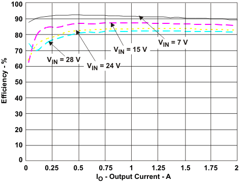 Figure 11. Efficiency
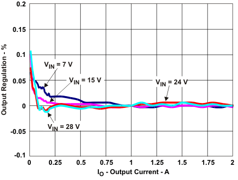 Figure 13. Load Regulation
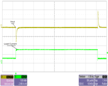 Figure 15. Transient Response
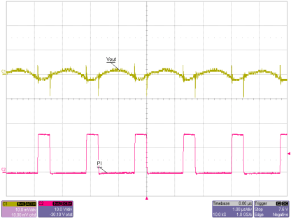 Figure 17. Output Ripple
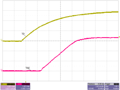 Figure 19. Startup
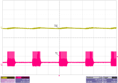 Figure 21. Eco-mode
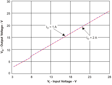
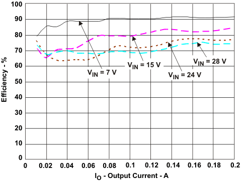 Figure 12. Low Current Efficiency
 Figure 14. Line Regulation
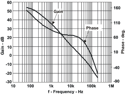 Figure 16. Loop Response
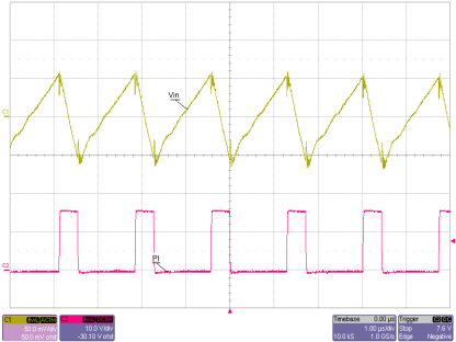 Figure 18. Input Ripple
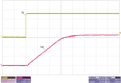
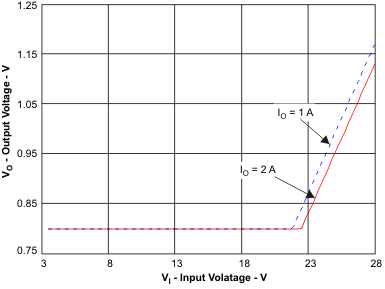 Figure 22. Typical Minimum Output Voltage vs Input Voltage