ZHCSED0 November 2015 TPS40210-EP
PRODUCTION DATA.
- 1 特性
- 2 应用
- 3 说明
- 4 修订历史记录
- 5 Pin Configuration and Functions
- 6 Specifications
-
7 Detailed Description
- 7.1 Overview
- 7.2 Functional Block Diagram
- 7.3
Feature Description
- 7.3.1 Soft-Start
- 7.3.2 BP Regulator
- 7.3.3 Shutdown (DIS/EN Pin)
- 7.3.4 Minimum On-Time and Off-Time Considerations
- 7.3.5 Setting the Oscillator Frequency
- 7.3.6 Synchronizing the Oscillator
- 7.3.7 Current Sense and Overcurrent
- 7.3.8 Current Sense and Subharmonic Instability
- 7.3.9 Current Sense Filtering
- 7.3.10 Control Loop Considerations
- 7.3.11 Gate Drive Circuit
- 7.4 Device Functional Modes
-
8 Application and Implementation
- 8.1 Application Information
- 8.2
Typical Application
- 8.2.1 Design Requirements
- 8.2.2
Detailed Design Procedure
- 8.2.2.1 Duty Cycle Estimation
- 8.2.2.2 Inductor Selection
- 8.2.2.3 Rectifier Diode Selection
- 8.2.2.4 Output Capacitor Selection
- 8.2.2.5 Input Capacitor Selection
- 8.2.2.6 Current Sense and Current Limit
- 8.2.2.7 Current Sense Filter
- 8.2.2.8 Switching MOSFET Selection
- 8.2.2.9 Feedback Divider Resistors
- 8.2.2.10 Error Amplifier Compensation
- 8.2.2.11 RC Oscillator
- 8.2.2.12 Soft-Start Capacitor
- 8.2.2.13 Regulator Bypass
- 8.2.2.14 Bill of Materials
- 8.2.3 Application Curves
- 9 Power Supply Recommendations
- 10Layout
- 11器件和文档支持
- 12机械、封装和可订购信息
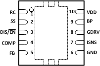
5 Pin Configuration and Functions
DRC Surface Mount Package
10-Pin VSON
Top View

Pin Functions
| PIN | I/O | DESCRIPTION | |
|---|---|---|---|
| NAME | NO. | ||
| BP | 9 | O | Regulator output pin. Connect a 1.0-μF bypass capacitor from this pin to GND. |
| COMP | 4 | O | Error amplifier output. Connect control loop compensation network between COMP pin and FB pin. |
| DIS/EN | 3 | I | Disable pin. Pulling this pin high, places the part into a shutdown mode. Shutdown mode is characterized by a very low quiescent current. While in shutdown mode, the functionality of all blocks is disabled and the BP regulator is shut down. This pin has an internal 1 MΩ pull-down resistor to GND. Leaving this pin unconnected enables the device. |
| FB | 5 | I | Error amplifier inverting input. Connect a voltage divider from the output to this pin to set output voltage. Compensation network is connected between this pin and COMP. |
| GDRV | 8 | O | Connect the gate of the power N channel MOSFET to this pin. |
| GND | 6 | — | Device ground. |
| ISNS | 7 | I | Current sense pin. Connect an external current sensing resistor between this pin and GND. The voltage on this pin is used to provide current feedback in the control loop and detect an overcurrent condition. An overcurrent condition is declared when ISNS pin voltage exceeds the overcurrent threshold voltage, 150 mV typical. |
| RC | 1 | I | Switching frequency setting pin. Connect a resistor from RC pin to VDD of the IC power supply and a capacitor from RC to GND. |
| SS | 2 | I | Soft-start time programming pin. Connect capacitor from SS pin to GND to program converter soft-start time. This pin also functions as a timeout timer when the power supply is in an overcurrent condition. |
| VDD | 10 | I | System input voltage. Connect a local bypass capacitor from this pin to GND. Depending on the amount of required slope compensation, this pin can be connected to the converter output. See Application Information for additional details. |