ZHCSED0 November 2015 TPS40210-EP
PRODUCTION DATA.
- 1 特性
- 2 应用
- 3 说明
- 4 修订历史记录
- 5 Pin Configuration and Functions
- 6 Specifications
-
7 Detailed Description
- 7.1 Overview
- 7.2 Functional Block Diagram
- 7.3
Feature Description
- 7.3.1 Soft-Start
- 7.3.2 BP Regulator
- 7.3.3 Shutdown (DIS/EN Pin)
- 7.3.4 Minimum On-Time and Off-Time Considerations
- 7.3.5 Setting the Oscillator Frequency
- 7.3.6 Synchronizing the Oscillator
- 7.3.7 Current Sense and Overcurrent
- 7.3.8 Current Sense and Subharmonic Instability
- 7.3.9 Current Sense Filtering
- 7.3.10 Control Loop Considerations
- 7.3.11 Gate Drive Circuit
- 7.4 Device Functional Modes
-
8 Application and Implementation
- 8.1 Application Information
- 8.2
Typical Application
- 8.2.1 Design Requirements
- 8.2.2
Detailed Design Procedure
- 8.2.2.1 Duty Cycle Estimation
- 8.2.2.2 Inductor Selection
- 8.2.2.3 Rectifier Diode Selection
- 8.2.2.4 Output Capacitor Selection
- 8.2.2.5 Input Capacitor Selection
- 8.2.2.6 Current Sense and Current Limit
- 8.2.2.7 Current Sense Filter
- 8.2.2.8 Switching MOSFET Selection
- 8.2.2.9 Feedback Divider Resistors
- 8.2.2.10 Error Amplifier Compensation
- 8.2.2.11 RC Oscillator
- 8.2.2.12 Soft-Start Capacitor
- 8.2.2.13 Regulator Bypass
- 8.2.2.14 Bill of Materials
- 8.2.3 Application Curves
- 9 Power Supply Recommendations
- 10Layout
- 11器件和文档支持
- 12机械、封装和可订购信息
10 Layout
10.1 Layout Guidelines
- For the maximum effectiveness from C9, place it near the VDD pin of the controller. Excessive high frequency noise on VDD during switching degrades overall regulation as the load increases.
- Keep the output loop (Q1-D1-C12-R11) as small as possible. A larger loop can degrade current limit accuracy and increase rediated emissions.
- For best current limit accuracy keep the ISNS filter components C10 and R10 near the ISNS and GND pins.
- Avoid connecting traces carrying large AC currents through a ground plane. Instead, use PCB traces on the top layer to conduct the AC current and use the ground plane as a noise shield.
- Split the ground plane as necessary to keep noise away from the TPS40210-EP and noise sensitive areas such as components connected to the RC pin, FB pin, COMP pin and SS pin. Also keep these noise sensitive components close to the TPS40210-EP IC.
- Keep C7 near the BP and GND pins to provide good bypass for the BP regulator.
- The GDRV trace should be as close as possible to the power FET gate to minimize parisitic resistance and inductance in the trace. The parasitics should also be minimized in the return path from the source of the MOSFET, through the sense resistor and back to the GND pin.
- Keep the SW node as physically small as possible to minimize parasitic capacitance and radiated emissions.
- For good output voltage regulation, Kelvin connections should be brought from the load to the top FB resistor R7.
10.2 Layout Example
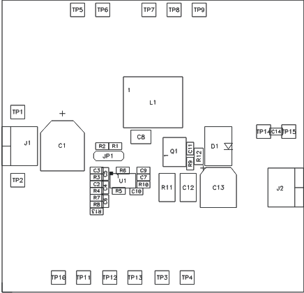 Figure 35. Component Placement
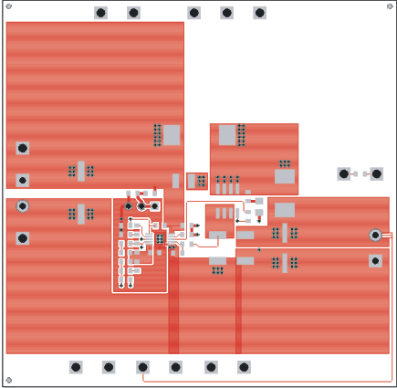 Figure 36. Top Copper
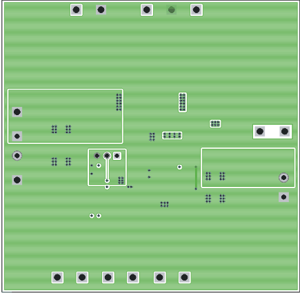 Figure 37. Bottom Copper Viewed from Top
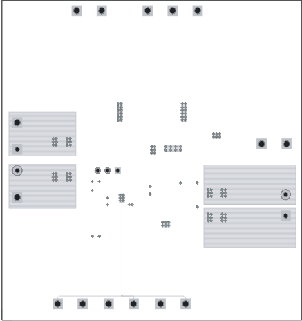 Figure 38. Internal 1 Copper Viewed from Top
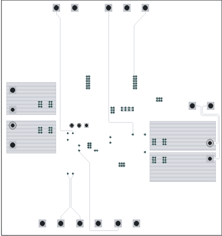 Figure 39. Internal 2 Copper Viewed from Top