ZHCSJQ2A May   2019  – August 2019 TPS2596

PRODUCTION DATA.  

  1. 特性
  2. 应用
  3. 说明
    1.     Device Images
      1.      简化原理图
      2.      TPS25963x 1KV EFT 响应
  4. 修订历史记录
  5. 器件比较表
  6. Pin Configuration and Functions
    1.     Pin Functions
  7. Specifications
    1. 7.1 Absolute Maximum Ratings
    2. 7.2 ESD Ratings
    3. 7.3 Recommended Operating Conditions
    4. 7.4 Thermal Information
    5. 7.5 Electrical Characteristics
    6. 7.6 Timing Requirements
    7. 7.7 Switching Characteristics
    8. 7.8 Typical Characteristics
  8. Detailed Description
    1. 8.1 Overview
    2. 8.2 Functional Block Diagram
    3. 8.3 Feature Description
      1. 8.3.1 Undervoltage Protection (UVP) and Undervoltage Lockout (UVLO)
      2. 8.3.2 Overvoltage Protection
        1. 8.3.2.1 Overvoltage Lockout
        2. 8.3.2.2 Overvoltage Clamp
      3. 8.3.3 Inrush Current, Overcurrent and Short Circuit Protection
        1. 8.3.3.1 Slew Rate and Inrush Current Control (dVdt)
        2. 8.3.3.2 Active Current Limiting
        3. 8.3.3.3 Short-Circuit Protection
      4. 8.3.4 Analog Load Current Monitor (IMON)
      5. 8.3.5 Overtemperature Protection (OTP)
      6. 8.3.6 Fault Indication
    4. 8.4 Device Functional Modes
      1. 8.4.1 Enable and Fault Pin Functional Mode 1: Single Device, Self-Controlled
      2. 8.4.2 Enable and Fault Pin Functional Mode 2: Single Device, Host-Controlled
      3. 8.4.3 Enable and Fault Pin Functional Mode 3: Multiple Devices, Self-Controlled
  9. Application and Implementation
    1. 9.1 Application Information
    2. 9.2 Typical Application
      1. 9.2.1 Precision Current Limiting and Protection for White Goods
      2. 9.2.2 Design Requirements
      3. 9.2.3 Detailed Design Procedure
        1. 9.2.3.1 Programming the Current-Limit Threshold: RILM Selection
        2. 9.2.3.2 Undervoltage and Overvoltage Lockout Set Point
        3. 9.2.3.3 Setting Output Voltage Ramp Time (TdVdT)
          1. 9.2.3.3.1 Case 1: Start-Up Without Load. Only Output Capacitance COUT Draws Current
          2. 9.2.3.3.2 Case 2: Start-Up With Load. Output Capacitance COUT and Load Draw Current
      4. 9.2.4 Support Component Selection: RFLT and CIN
      5. 9.2.5 Application Curves
    3. 9.3 System Examples
      1. 9.3.1 Current Limiting and Overvoltage Protection and for Energy Meter Power Rails
      2. 9.3.2 Precision Current Limiting and Protection in Appliances
  10. 10Power Supply Recommendations
    1. 10.1 Transient Protection
    2. 10.2 Output Short-Circuit Measurements
  11. 11Layout
    1. 11.1 Layout Guidelines
    2. 11.2 Layout Example
  12. 12器件和文档支持
    1. 12.1 文档支持
      1. 12.1.1 相关文档
    2. 12.2 接收文档更新通知
    3. 12.3 社区资源
    4. 12.4 商标
    5. 12.5 静电放电警告
    6. 12.6 Glossary
  13. 13机械、封装和可订购信息

封装选项

机械数据 (封装 | 引脚)
散热焊盘机械数据 (封装 | 引脚)
订购信息

Overvoltage Lockout

The TPS25963x variants provide an user adjustable OVLO mechanism to ensure that the supply to the load is cut off if the input supply voltage exceeds a certain level. This can be achieved by dividing the input supply and feeding it to the OVLO pin. Whenever the voltage at the OVLO pin rises above a threshold VOVLO(R), the device turns OFF the FET. When the voltage at the OVLO pin falls below the threshold VOVLO(F), the FET is turned ON again. The rising and falling thresholds on this pin are slightly different, thereby providing some hysteresis and ensuring stable operation around the threshold voltage.
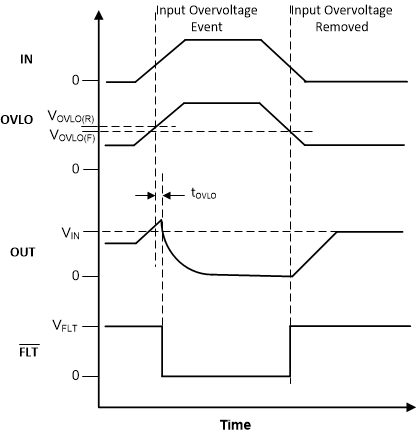
TPS2596 Timing-diagram-OVLO.gifFigure 45. TPS25963x Overvoltage Lockout Response

The user should choose the resistor divider values appropriately to map the desired input overvoltage level to the OVLO threshold of the part.
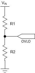
TPS2596 Circuit-OVLO-connection-TPS25963x.gifFigure 46. TPS25963x Adjustable Overvoltage Lockout
Equation 2. TPS2596 Equation-OVLO.gif