ZHCSCQ0 August 2014 TPS25921A , TPS25921L
PRODUCTION DATA.
- 1 特性
- 2 应用范围
- 3 说明
- 4 应用电路原理图
- 5 修订历史记录
- 6 Pin Configuration and Functions
- 7 Specifications
- 8 Parametric Measurement Information
-
9 Detailed Description
- 9.1 Overview
- 9.2 Functional Block Diagram
- 9.3 Feature Description
- 9.4 Device Functional Modes
-
10Applications and Implementation
- 10.1 Application Information
- 10.2
Typical Application
- 10.2.1
Precision Current Limiting and Protection for White Goods
- 10.2.1.1 Design Requirements
- 10.2.1.2 Detailed Design Procedure
- 10.2.1.3 Application Curves
- 10.2.1
Precision Current Limiting and Protection for White Goods
- 11System Examples
- 12Power Supply Recommendations
- 13Layout
- 14器件和文档支持
- 15机械封装和可订购信息
9 Detailed Description
9.1 Overview
TPS25921 is a smart eFuse with enhanced built-in protection circuitry. It provides robust protection for all systems and applications powered from 4.5 V to 18 V.
For hot-plug-in boards, the device provides in-rush current control and programmable output ramp-rate. TPS25921 integrates overcurrent and short circuit protection. The precision overcurrent limit helps to minimize over design of the input power supply, while the fast response short circuit protection immediately isolates the load from input when a short circuit is detected. The device allows the user to program the overcurrent limit threshold between 0.4 A and 1.6 A via an external resistor. The device provides precise monitoring of voltage bus for brown-out and overvoltage conditions and asserts fault for downstream system. Its threshold accuracy of 3% ensures tight supervision of bus, eliminating the need for a separate supply voltage supervisor chip. TPS25921 is designed to protect systems such as White Goods, STBs, DTVs, Smart Meters and Gas Analyzers.
The additional features include:
- Over temperature protection to safely shutdown in the event of an overcurrent event
- Fault reporting for brown-out and overvoltage faults
- A choice of latched or automatic restart mode
9.2 Functional Block Diagram
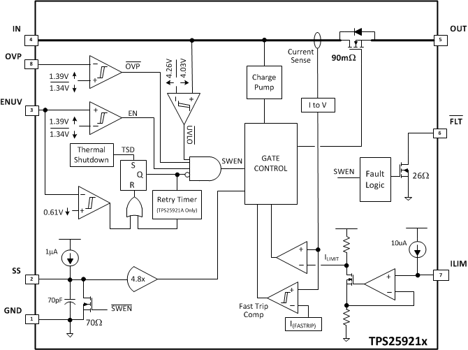
9.3 Feature Description
9.3.1 Enable and Adjusting Undervoltage Lockout (UVLO)
The ENUV pin controls the ON/OFF state of the internal FET. A voltage V(ENUV) < V(ENF) on this pin turns off the internal FET, thus disconnecting IN from OUT.
Toggling the ENUV pin below V(ENF_RST) resets the TPS25921L that has latched off due to a fault condition. The internal de-glitch delay on ENUV falling edge is kept low for quick detection of power failure. For applications where a higher de-glitch delay on ENUV is desired, or when the supply is particularly noisy, it is recommended to use an external filter capacitor from the ENUV terminal to GND.
The undervoltage lockout threshold can be programmed by using an external resistor divider from the supply IN terminal to the ENUV terminal to GND as shown in Figure 26. When an undervoltage or input power fail event is detected, the internal FET is quickly turned off, and FLT is asserted. If the undervoltage lockout function is not needed, the ENUV pin should be connected to the IN terminal. The ENUV terminal should not be left floating.
TPS25921 also implements internal undervoltage lockout (UVLO) circuitry on the IN pin. The device gets disabled when the IN terminal voltage falls below internal UVLO Threshold V(UVF).
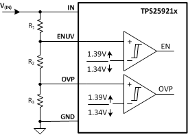 Figure 26. UVLO and OVP Thresholds Set By R1, R2 and R3
9.3.2 Overvoltage Protection (OVP)
TPS25921 incorporates circuits to protect the system during overvoltage conditions. A resistor divider, connected from the supply to OVP terminal to GND (as shown in Figure 26), programs the overvoltage threshold. A voltage more than V(OVPR) on the OVP pin turns off the internal FET and protects the downstream load. This pin should be tied to GND when not used.
9.3.3 Hot Plug-in and In-Rush Current Control
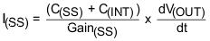
TPS25921 is designed to control the in-rush current upon insertion of a card into a live backplane or other "hot" power source. This limits the voltage sag on the backplane’s supply voltage and prevents unintended resets of the system power. A slew rate controlled startup (SS) also helps to eliminate conductive and radiated interference. An external capacitor from the SS pin to GND defines the slew rate of the output voltage at power-on (as shown in Figure 27). The equation governing slew rate at start-up is shown in Equation 1 :
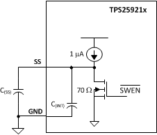 Figure 27. Output Ramp Up Time tdVdT is Set by C(dVdT)
Where:
- I(SS) = 1 µA (typical)
-
 = Desired output slew rate
 - GAIN(SS) = ΔV(OUT)/ΔV(SS) gain = 4.85
The total ramp time (tSS) of V(OUT) for 0 to V(IN) can be calculated using Equation 2:
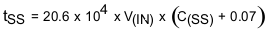
The inrush current, I(INRUSH) can be calculated as
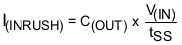
The SS pin can be left floating to obtain a predetermined slew rate (tSS) on the output. When terminal is left floating, the device sets an internal ramp rate of ~50V/ms for output (V(OUT)) ramp.
Figure 36 and Figure 37 illustrate the inrush current control behavior of the device. For systems where load is present during start-up, the current never exceeds the overcurrent limit set by R(ILIM) resistor for the application. For defining appropriate charging time/rate under different load conditions, refer to the Setting Output Voltage Ramp time (tSS) section.
9.3.4 Overload and Short Circuit Protection :
At all times load current is monitored by sensing voltage across an internal sense resistor. During overload events, current is limited to the current limit (ILIMIT) programmed by R(ILIM) resistor

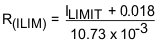
- ILIMIT is overload current limit in Ampere
- R(ILIM) is the current limit programming resistor in kΩ
TPS25921 incorporates two distinct overcurrent protection levels: the current limit (ILIMIT) and the fast-trip threshold (I(FASTRIP)). The fast trip and current limit operations are shown in Figure 28.
Bias current on ILIM pin directly controls current-limiting behavior of the device, and PCB routing of this node must be kept away from any noisy (switching) signals.
9.3.4.1 Overload Protection
For overload conditions, the internal current-limit amplifier regulates the output current to ILIMIT. The output voltage droops during current limit regulation, resulting in increased power dissipation in the device. If the device junction temperature reaches the thermal shutdown threshold (T(TSD)), the internal FET is turned off. Once in thermal shutdown, The TPS25921L version stays latched off, whereas TPS25921A commences an auto-retry cycle tTSD(dly) ms after TJ < [T(TSD) - 20°C]. During thermal shutdown, the fault pin FLT pulls low to signal a fault condition. Figure 40 and Figure 41 illustrate overload behavior.
9.3.4.2 Short Circuit Protection
During a transient short circuit event, the current through the device increases very rapidly. As current-limit amplifier cannot respond quickly to this event due to its limited bandwidth, the device incorporates a fast-trip comparator, with a threshold I(FASTRIP). When the current through the internal FET exceeds I(FASTRIP) (I(OUT) > I(FASTRIP)), this comparator shuts down the pass device within 3 µs and terminates the rapid short-circuit peak current. The I(FASTRIP) threshold is dependent on programmed overload current limit and function of R(ILIM). See Equation 6 for the calculation.

where
- I(FASTRIP) is fast trip current limit in Ampere
- R(ILIM) is the current limit resistor in kΩ
The fast-trip circuit holds the internal FET off for only a few microseconds, after which the device attempts to turn back on normally, allowing the current-limit loop to regulate the output current to ILIMIT. Then, device behaves similar to overload condition. Figure 42 through Figure 44 illustrate the behavior of the system when the current exceeds the fast-trip threshold.
9.3.4.3 Start-Up with Short on Output
During start-up into a short circuit current is limited to ILIMIT. Figure 45 and Figure 46 illustrate start-up with a short on the output. This feature helps in quick fault isolation and hence ensures stability of the DC bus.
9.3.4.4 Constant Current Limit Behavior during Overcurrent Faults
When power dissipation in the internal FET [PD = (V(IN) - V(OUT)) × I(OUT)] > 2 W, there is a ~1 to 20 % thermal fold back in the current limit value so that the regulated current drops from ILIMIT to IOS. Eventually, the device shuts down due to over temperature.
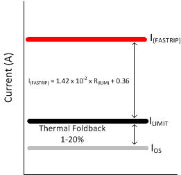 Figure 28. Overcurrent Protection Levels
9.3.5 FAULT Response
The FLT open-drain output is asserted (active low) during undervoltage, overvoltage and thermal shutdown conditions. The FLT signal remains asserted until the fault condition is removed and the device resumes normal operation. During thermal shutdown, TPS25921L version stays latched off, whereas TPS25921A commences an auto-retry cycle tTSD(dly) millisecond after TJ < [T(TSD) - 20°C]. For TPS25921L, thermal fault latch can be reset by cycling the ENUV pin below V(ENF_RST) threshold. A nuisance fast trip does not trigger fault.
Connect FLT with a pull up resistor to Input or Output voltage rail. FLT may be left open or tied to ground when not used.
9.3.6 IN, OUT and GND Pins
The IN pin should be connected to the power source. A ceramic bypass capacitor close to the device from IN to GND is recommended to alleviate bus transients. The recommended operating voltage range is 4.5 V – 18 V.
The OUT pin should be connected to the load. V(OUT) in the ON condition, is calculated using the Equation 7
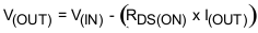
where, RDS(ON) is the ON resistance of the internal FET.
GND terminal is the most negative voltage in the circuit and is used as a reference for all voltage reference unless otherwise specified.
9.3.7 Thermal Shutdown:
Internal over temperature shutdown disables/turns off the FET when TJ > 155°C (typical). The TPS25921L version latches off the internal FET, whereas TPS25921A commences an auto-retry cycle tTSD(dly) milliseconds after TJ drops below [T(TSD) - 20°C]. During the thermal shutdown, the fault pin FLT is pulled low to signal a fault condition.
9.4 Device Functional Modes
9.4.1 Shutdown Control
The internal FET and hence the load current can be remotely switched off by taking the ENUV pin below its 1.34 V threshold with an open collector or open drain device as shown in Figure 29. Upon releasing the ENUV pin the device turns on with soft-start cycle.
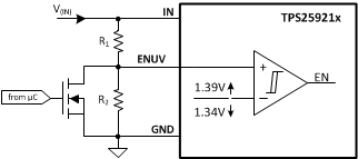 Figure 29. Shutdown Control
9.4.2 Operational Overview of Device Functions
The Table 1 below elucidates the device functionality for various conditions
Table 1. Operational Overview of Device Functions
| Device | TPS25921 |
|---|---|
| Start Up | Inrush ramp controlled by capacitor at SS pin |
| Inrush limited to ILIMIT level as set by R(ILIM) | |
| If TJ > T(TSD) device shuts off | |
| Overcurrent Response | Current is limited to I(LIM) level as set by R(ILIM) |
| Power dissipation increases as V(IN) - V(OUT) grows | |
| Device turns off when TJ > T(TSD) | |
| ‘L' Version remains off | |
| 'A' Version will attempt restart tTSD(dly) ms after TJ < [T(TSD) -20°C] | |
| Short-Circuit Response | Fast shut off when I(LOAD) > I(FASTRIP) |
| Quick restart and current limited to ILIMIT, follows standard startup cycle |