ZHCSCQ0 August 2014 TPS25921A , TPS25921L
PRODUCTION DATA.
- 1 特性
- 2 应用范围
- 3 说明
- 4 应用电路原理图
- 5 修订历史记录
- 6 Pin Configuration and Functions
- 7 Specifications
- 8 Parametric Measurement Information
-
9 Detailed Description
- 9.1 Overview
- 9.2 Functional Block Diagram
- 9.3 Feature Description
- 9.4 Device Functional Modes
-
10Applications and Implementation
- 10.1 Application Information
- 10.2
Typical Application
- 10.2.1
Precision Current Limiting and Protection for White Goods
- 10.2.1.1 Design Requirements
- 10.2.1.2 Detailed Design Procedure
- 10.2.1.3 Application Curves
- 10.2.1
Precision Current Limiting and Protection for White Goods
- 11System Examples
- 12Power Supply Recommendations
- 13Layout
- 14器件和文档支持
- 15机械封装和可订购信息
7 Specifications
7.1 Absolute Maximum Ratings
over operating free-air temperature range (unless otherwise noted) (1)| VALUE(2) | UNIT | |||
|---|---|---|---|---|
| MIN | MAX | |||
| Input voltage range | IN, OUT, ENUV, OVP, FLT | –0.3 | 20 | V |
| IN (10 ms Transient) | 22 | |||
| ILIM, SS | –0.3 | 7 | ||
| Sink current | SS | 5 | mA | |
| FLT | 100 | mA | ||
| Source current | ILIM, SS, FLT | Internally Limited | ||
| Maximum junction temperature, TJ | Internally Limited | °C | ||
(1) Stresses beyond those listed under absolute maximum ratings may cause permanent damage to the device. These are stress ratings only and functional operation of the device at these or any conditions beyond those indicated under recommended operating conditions is not implied. Exposure to absolute-maximum-rated conditions for extended periods may affect device reliability.
(2) All voltage values, except differential voltages, are with respect to network ground terminal.
7.2 Handling Ratings
| MIN | MAX | UNIT | |||
|---|---|---|---|---|---|
| Tstg | Storage temperature range | -65 | 150 | °C | |
| V(ESD) | Electrostatic discharge | Human body model (HBM), per ANSI/ESDA/JEDEC JS-001, all pins(1) | –2 | 2 | kV |
| Charged device model (CDM), per JEDEC specification JESD22-C101, all pins(2) | –0.5 | 0.5 | |||
(1) JEDEC document JEP155 states that 500-V HBM allows safe manufacturing with a standard ESD control process.
(2) JEDEC document JEP157 states that 250-V CDM allows safe manufacturing with a standard ESD control process.
7.3 Recommended Operating Conditions
over operating free-air temperature range (unless otherwise noted)| MIN | TYP | MAX | UNIT | ||
|---|---|---|---|---|---|
| Input voltage range | IN | 4.5 | 18 | V | |
| OUT, OVP, ENUV, FLT | 0 | 18 | |||
| SS | 0 | 6 | |||
| ILIM | 0 | 3.3 | |||
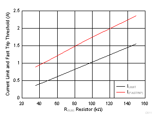
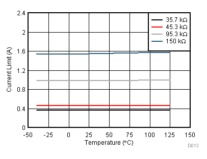
| Resistance | ILIM | 35.7 | 95.3 | 158 | kΩ |
| External capacitance | OUT | 0.1 | 1 | µF | |
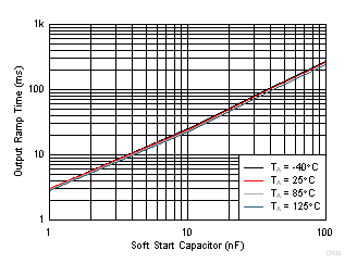
| SS | 1 | 1000 | nF | ||
| Operating junction temperature range, TJ | –40 | 25 | 125 | °C | |
7.4 Thermal Characteristics(1)
| THERMAL METRIC | TPS2592xx | UNIT | |
|---|---|---|---|
| SOIC (8) PINS | |||
| RθJA | Junction-to-ambient thermal resistance | 120.8 | °C/W |
| RθJCtop | Junction-to-case (top) thermal resistance | 65.5 | |
| RθJB | Junction-to-board thermal resistance | 51.8 | |
| ψJT | Junction-to-top characterization parameter | 17.4 | |
| ψJB | Junction-to-board characterization parameter | 61.2 | |
(1) For more information about traditional and new thermal metrics, see the IC Package Thermal Metrics application report, SPRA953.
7.5 Electrical Characteristics
Conditions (unless otherwise noted) are –40°C ≤ TJ ≤ 125°C, 4.5 V ≤ V(IN) ≤ 18 V, V(ENUV) = 2 V, V(OVP) = 0 V, R(ILIM) = 95.3 kΩ, CSS = OPEN, FLT = OPEN. Positive current into terminals. All voltages are referenced to GND (unless otherwise noted).| PARAMETER | TEST CONDITIONS | MIN | TYP | MAX | UNIT | |
|---|---|---|---|---|---|---|
| SUPPLY VOLTAGE AND INTERNAL UNDERVOLTAGE LOCKOUT | ||||||
| V(IN) | Operating Input Voltage | 4.5 | 18 | V | ||
| V(UVR) | UVLO Threshold, Rising | 4.10 | 4.26 | 4.40 | V | |
| V(UVHys) | UVLO Hysteresis | 168 | 224 | 279 | mV | |
| IQ(ON) | Supply Current, Enabled | V(ENUV) = 2 V, V(IN) = 12 V | 0.22 | 0.41 | 0.58 | mA |
| IQ(OFF) | Supply Current, Disabled | V(ENUV) = 0 V, V(IN) = 12 V | 0.08 | 0.132 | 0.20 | mA |
| OVERVOLTAGE PROTECTION (OVP) INPUT | ||||||
| V(OVPR) | Overvoltage Threshold Voltage, Rising | 1.35 | 1.39 | 1.43 | V | |
| V(OVPF) | Overvoltage Threshold Voltage, Falling | 1.30 | 1.34 | 1.37 | V | |
| I(OVP) | OVP Input Leakage Current | 0V ≤ V(OVP) ≤ 18 V | –100 | 0 | 100 | nA |
| ENABLE AND UNDERVOLTAGE LOCKOUT (ENUV) INPUT | ||||||
| V(ENR) | ENUV Threshold voltage, rising | 1.36 | 1.39 | 1.42 | V | |
| V(ENF) | ENUV Threshold voltage, falling | 1.30 | 1.34 | 1.37 | V | |
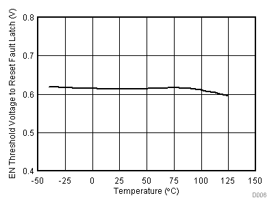
| V(ENF_RST) | ENUV Threshold voltage to reset thermal fault, falling | 0.5 | 0.61 | 0.8 | V | |
| IEN | EN Input leakage current | 0 ≤ V(ENUV) ≤ 18 V | –100 | 0 | 100 | nA |
| SOFT START: OUTPUT RAMP CONTROL (SS) | ||||||
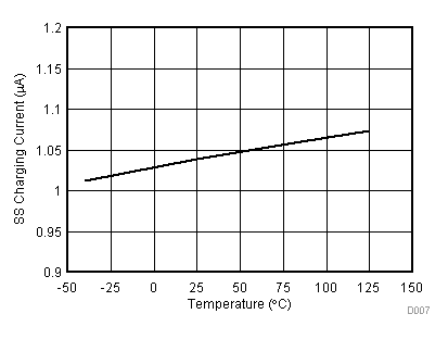
| I(SS) | SS charging current | V(SS) = 0 V | 0.9 | 1.04 | 1.2 | µA |
| R(SS) | SS discharging resistance | V(ENUV) = 0 V, I(SS) = 10 mA sinking | 60 | 70 | 85 | Ω |
| V(SSmax) | SS maximum capacitor voltage | 5.5 | V | |||
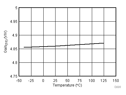
| GAIN(SS) | SS to OUT gain | ΔV(OUT)/ΔV(SS) | 4.81 | 4.86 | 4.92 | V/V |
| CURRENT LIMIT PROGRAMMING (ILIM) | ||||||
| I(ILIM) | ILIM Bias current | 6 | 10 | 16 | µA | |
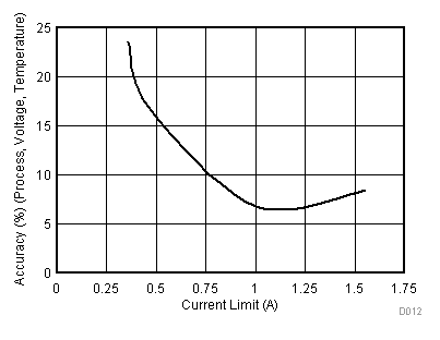
| ILIMIT | Current Limit(2) | R(ILIM) = 35.7 kΩ, (V(IN) - V(OUT)) = 1 V | 0.284 | 0.368 | 0.452 | A |
| R(ILIM) = 45.3 kΩ, (V(IN) - V(OUT)) = 1 V | 0.394 | 0.471 | 0.547 | |||
| R(ILIM) = 95.3 kΩ, (V(IN) - V(OUT)) = 1 V, TA = TJ= 25°C | 0.98 | 1.0 | 1.02 | |||
| R(ILIM) = 95.3 kΩ, (V(IN) - V(OUT)) = 1 V | 0.93 | 1.0 | 1.062 | |||
| R(ILIM) = 150 kΩ, (V(IN) - V(OUT)) = 1 V | 1.43 | 1.57 | 1.7 | |||
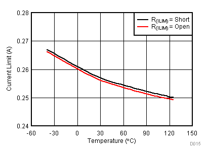
| R(ILIM) = SHORT, Shorted resistor current limit R(ILIM) = OPEN, Open resistor current limit (Single Point Failure Test: UL60950) |
0.12 | 0.257 | 0.406 | |||
| IOS | Short-circuit current limit(2) | R(ILIM) = 35.7 kΩ, (V(IN) - V(OUT)) = 12 V | 0.275 | 0.356 | 0.438 | A |
| R(ILIM) = 45.3 kΩ, (V(IN) - V(OUT)) = 12 V | 0.376 | 0.45 | 0.522 | |||
| R(ILIM) = 95.3 kΩ, (V(IN) - V(OUT)) = 12 V | 0.837 | 0.9 | 0.964 | |||
| R(ILIM) = 150 kΩ, (V(IN) - V(OUT)) = 12 V | 1.219 | 1.34 | 1.46 | |||
| I(FASTRIP) | Fast-Trip comparator threshold | R(ILIM) in kΩ | 0.0142 x R(ILIM) + 0.36 | A | ||
| V(ILIMopen) | ILIM Open resistor detect threshold | V(ILIM) Rising, R(ILIM) = OPEN | 2.81 | 3.0 | 3.25 | V |
| MOSFET – POWER SWITCH | ||||||
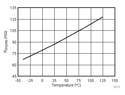
| RDS(on) |
FET ON resistance(1) |
–40°C ≤ TJ ≤ 85°C | 55 | 87 | 120 | mΩ |
| –40°C ≤ TJ ≤ 125°C | 55 | 87 | 135 | |||
| PASS FET OUTPUT (OUT) | ||||||
| Ilkg(OUT) | OUT Bias current in off state | V(ENUV) = 0 V, V(OUT) = 0 V (Sourcing) | –2 | 0 | 1 | µA |
| Isink(OUT) | V(ENUV) = 0V, V(OUT) = 300 mV (Sinking) | 5 | 7 | 10 | ||
| FAULT FLAG (FLT): ACTIVE LOW | ||||||
| R(FLT) | FLT Pull down Resistance | Device in fault condition, V(ENUV) = 0V, I(FLT) = 100mA | 22 | 26 | 32 | Ω |
| I(FLT) | FLT Input Leakage Current | Device not in fault condition, V(FLT) = 0V, 18V | –0.5 | 0 | 0.5 | µA |
| THERMAL SHUT DOWN (TSD) | ||||||
| T(TSD) | TSD Threshold, rising(1) | 155 | °C | |||
| T(TSDhys) | TSD Hysteresis(1) | 20 | °C | |||
| Thermal fault: Latched or Auto Retry | TPS25921L | LATCHED | ||||
| TPS25921A | AUTO-RETRY | |||||
(1) The limits for these parameters are specified based on design and characterization data, and are not tested during production.
(2) Pulse-testing techniques maintain junction temperature close to ambient temperature. Thermal effects must be taken into account separately.
7.6 Timing Requirements
Conditions (unless otherwise noted) are –40°C ≤ TJ ≤ 125°C, V(IN)= 12 V, V(ENUV) = 2 V, V(OVP) = 0 V, R(ILIM) = 95.3 kΩ, CSS = OPEN, FLT = OPEN. Positive current into terminals. All voltages are referenced to GND (unless otherwise noted). Refer to Figure 26 for the timing diagrams| MIN | TYP | MAX | UNIT | |||
|---|---|---|---|---|---|---|
| ENABLE AND UNDERVOLTAGE LOCKOUT (ENUV) INPUT | ||||||
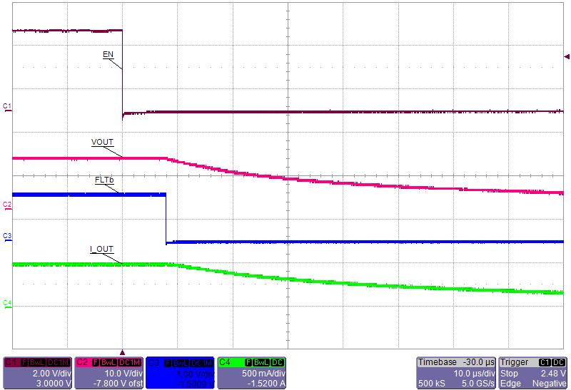
| tOFF(dly) | Turn Off delay | ENUV ↓ to V(OUT)↓ | 8 | µs | ||
| tON(dly) | Turn-On delay | ENUV ↑ to V(OUT) = 1V, C(SS) = OPEN |
96 | µs | ||
| ENUV ↑ to V(OUT) = 1V, C(SS) > 0.39nF, [C(dVdT) in nF] |
14.5 + 0.5 x ( 70p + C(SS)) | |||||
| OVERVOLTAGE PROTECTION (OVP) INPUT | ||||||
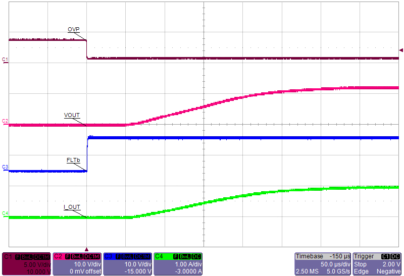
| tOVP(dly) | OVP Disable delay | OVP↑ to V(OUT)↓ | 8 | µs | ||
| SOFT START: OUTPUT RAMP CONTROL (SS) | ||||||
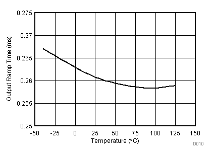
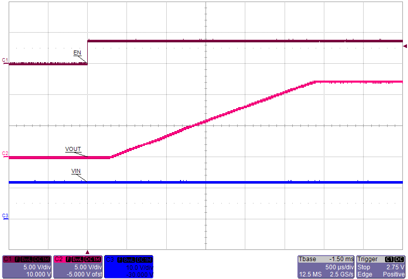
| tSS | Output ramp time | ENUV ↑ to V(OUT) = 11.7 V, with C(SS) = open , C(OUT) = 2.2 µF | 0.2 | 0.26 | 0.33 | ms |
| ENUV ↑ to V(OUT) = 11.7 V, with C(SS) = 1 nF, C(OUT) = 2.2 µF | 2.1 | 3 | 3.6 | |||
| CURRENT LIMIT PROGRAMMING (ILIM) | ||||||
| tFASTRIP(dly) | Fast-Trip comparator delay | I(OUT) > I(FASTRIP) | 3 | µs | ||
| THERMAL SHUT DOWN (TSD) | ||||||
| tTSD(dly) | Retry Delay after TSD recovery, TJ < [T(TSD) - 20oC] | TPS25921A Only, V(IN) = 12 V | 150 | ms | ||
| TPS25921A Only, V(IN) = 4.5 V | 100 | ms | ||||
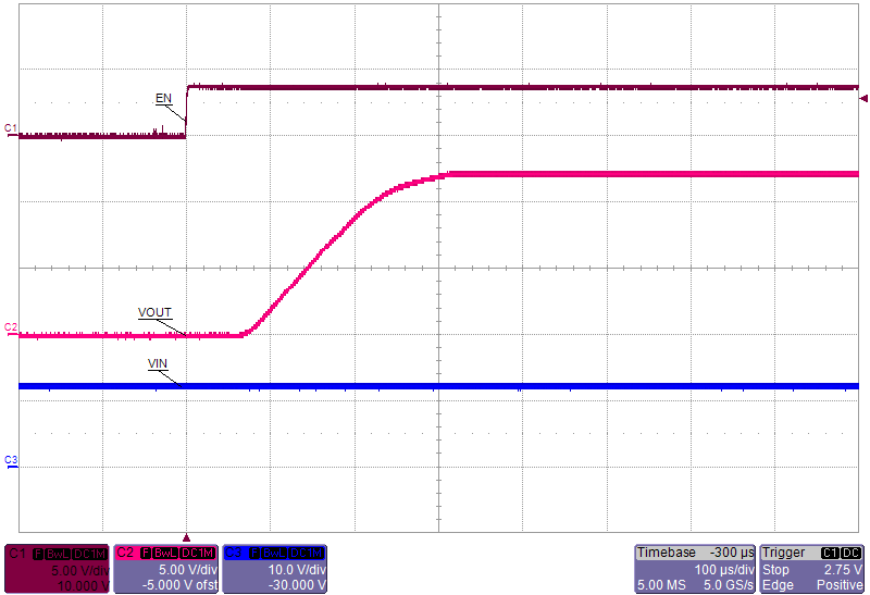
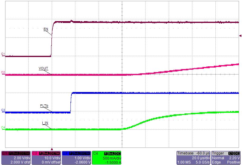
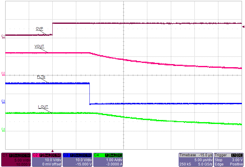
7.7 Typical Characteristics
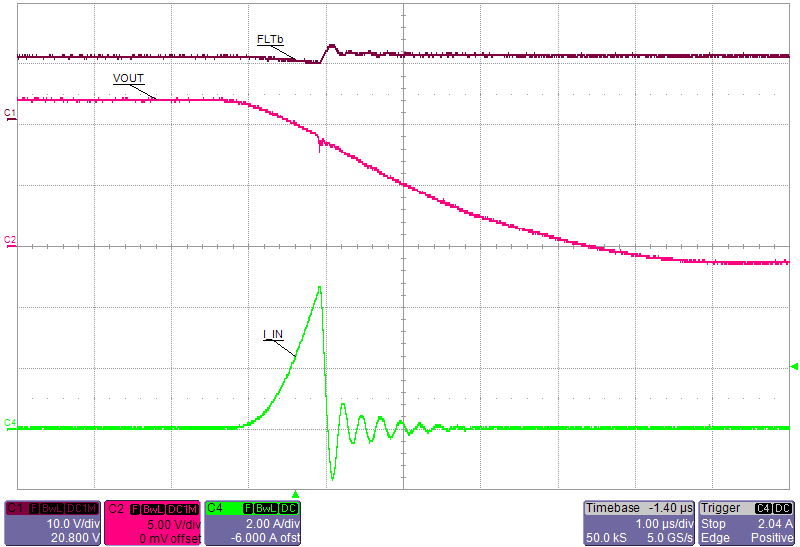
Conditions (unless otherwise noted) are –40°C ≤ TJ ≤ 125°C, V(IN)= 12 V, V(ENUV) = 2 V, V(OVP) = 0 V, R(ILIM) = 95.3 kΩ, C(OUT) = 2.2 μF, CSS = OPEN, FLT = OPEN. Positive current into terminals. All voltages referenced to GND (unless otherwise noted). For all oscilloscope waveforms TA = 25°C.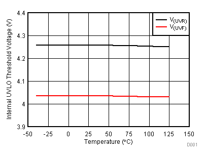 Figure 1. UVLO Threshold Voltage vs Temperature
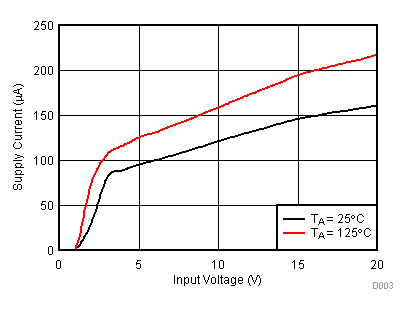 Figure 3. Input Supply Current vs Supply Voltage at Shutdown
| C(SS) = Open |
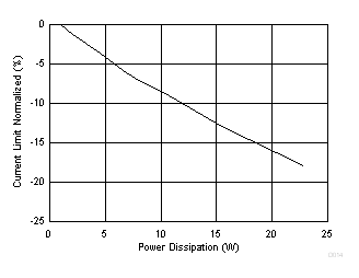
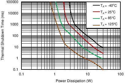
| PD = [V(IN)-V(OUT)]*ILIMIT |
| C(SS) = Open | C(OUT) = 4.7 nF |
| R(FLT) = 100 kΩ |
| RL = 12 Ω | R(FLT) = 100 kΩ |
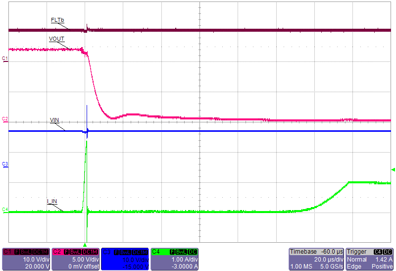
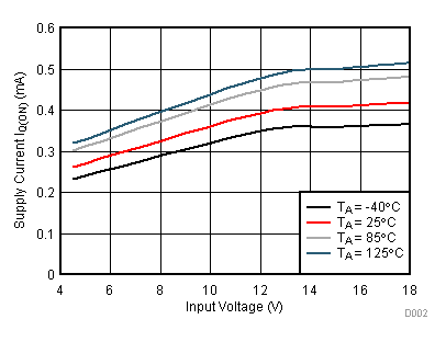 Figure 2. Input Supply Current vs Supply Voltage During Normal Operation
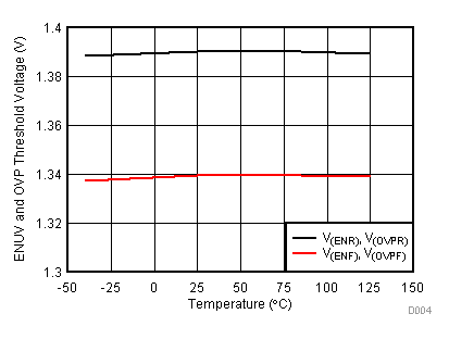 Figure 4. ENUV and OVP Threshold Voltage vs Temperature
| Taken on 1-Layer board, 2oz.(0.08-mm thick) with GND plane area: 14 cm2 (bottom) |
| C(SS) = 1nF | C(OUT) = 4.7 nF |
| R(FLT) = 100 kΩ |
| RL = 12 Ω | R(FLT) = 100 kΩ |