ZHCSCQ0 August 2014 TPS25921A , TPS25921L
PRODUCTION DATA.
- 1 特性
- 2 应用范围
- 3 说明
- 4 应用电路原理图
- 5 修订历史记录
- 6 Pin Configuration and Functions
- 7 Specifications
- 8 Parametric Measurement Information
-
9 Detailed Description
- 9.1 Overview
- 9.2 Functional Block Diagram
- 9.3 Feature Description
- 9.4 Device Functional Modes
-
10Applications and Implementation
- 10.1 Application Information
- 10.2
Typical Application
- 10.2.1
Precision Current Limiting and Protection for White Goods
- 10.2.1.1 Design Requirements
- 10.2.1.2 Detailed Design Procedure
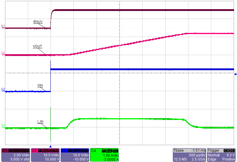
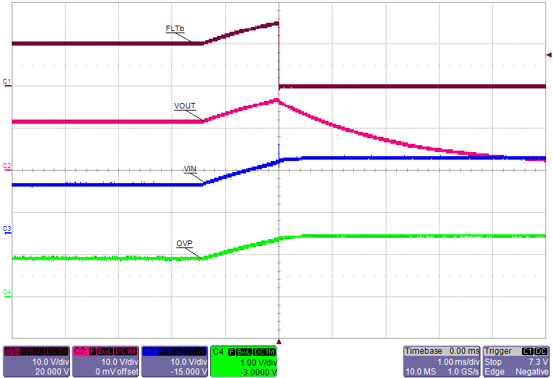
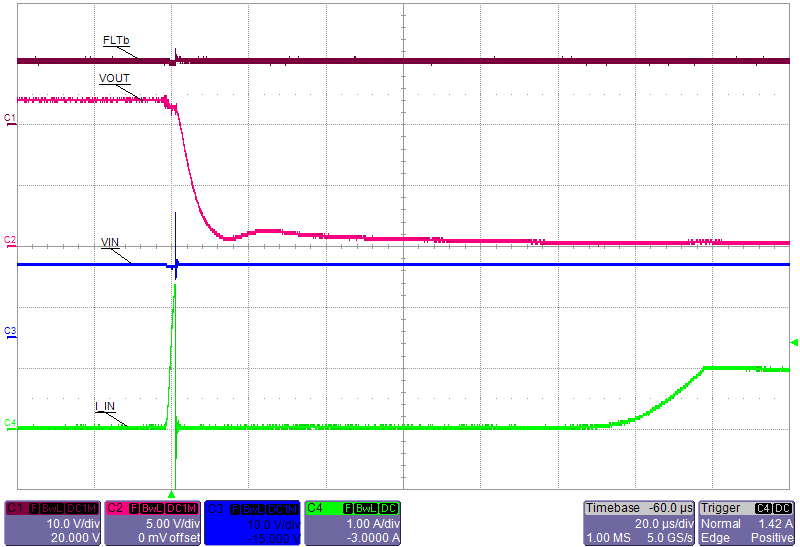
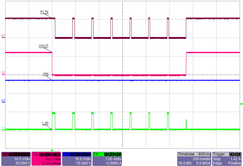
- 10.2.1.3 Application Curves
- 10.2.1
Precision Current Limiting and Protection for White Goods
- 11System Examples
- 12Power Supply Recommendations
- 13Layout
- 14器件和文档支持
- 15机械封装和可订购信息
10 Applications and Implementation
10.1 Application Information
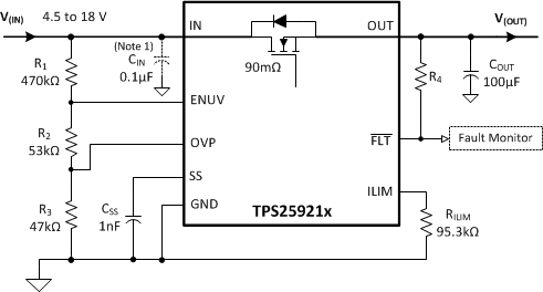
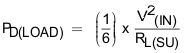
The TPS25921x is a smart eFuse. It is typically used for Hot-Swap and Power rail protection applications. It operates from 4.5 V to 18 V with programmable current limit, overvoltage and undervoltage protection. The device aids in controlling the in-rush current and provides precise current limiting during overload conditions for systems such as White Goods, Set-Top-Box, DTVs, Gaming Consoles, SSDs/HDDs and Smart Meters. The device also provides robust protection for multiple faults on the sub-system rail.
The following design procedure can be used to select component values for the device.
Alternatively, the WEBENCH® software may be used to generate a complete design. The WEBENCH® software uses an iterative design procedure and accesses a comprehensive database of components when generating a design. Additionally, a spreadsheet design tool TPS25921 Design Calculator is available on web folder.
This section presents a simplified discussion of the design process.
10.2 Typical Application
10.2.1 Precision Current Limiting and Protection for White Goods
10.2.1.1 Design Requirements
Table 2. Design Parameters
| DESIGN PARAMETER | EXAMPLE VALUE |
|---|---|
| Input voltage range, V(IN) | 12 V |
| Undervoltage lockout set point, V(UV) | 8 V |
| Overvoltage protection set point , V(OV) | 17 V |
| Load at Start-Up , RL(SU) | 24 Ω |
| Current limit, ILIMIT | 1 A |
| Load capacitance , C(OUT) | 100 µF |
| Maximum ambient temperatures , TA | 85°C |
10.2.1.2 Detailed Design Procedure
The following design procedure can be used to select component values for the TPS25921A and TPS25921L.
10.2.1.2.1 Step by Step Design Procedure
To begin the design process a few parameters must be decided upon. The designer needs to know the following:
- Normal input operation voltage
- Maximum output capacitance
- Maximum current Limit
- Load during start-up
- Maximum ambient temperature of operation
This design procedure below seeks to control the junction temperature of device under both static and transient conditions by proper selection of output ramp-up time and associated support components. The designer can adjust this procedure to fit the application and design criteria.
10.2.1.2.2 Programming the Current-Limit Threshold: R(ILIM) Selection
The R(ILIM) resistor at the ILIM pin sets the over load current limit, this can be set using Equation 5.
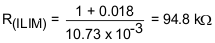
Choose closest standard value: 95.3 kΩ, 1% standard value resistor.
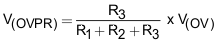
10.2.1.2.3 Undervoltage Lockout and Overvoltage Set Point
The undervoltage lockout (UVLO) and overvoltage trip point are adjusted using the external voltage divider network of R1, R2 and R3 as connected between IN, ENUV, OVP and GND pins of the device. The values required for setting the undervoltage and overvoltage are calculated solving Equation 9 and Equation 10.
For minimizing the input current drawn from the power supply {I(R123) = V(IN)/(R1 + R2 + R3)}, it is recommended to use higher values of resistance for R1, R2 and R3.
However, leakage currents due to external active components connected to the resistor string can add error to these calculations. So, the resistor string current, I(R123) must be chosen to be 20x greater than the leakage current expected.
From the device electrical specifications, V(OVPR) = 1.40 V and V(ENR) = 1.40 V. For design requirements, V(OV) is 17 V and V(UV) is 8 V. To solve the equation, first choose the value of R3 = 47 kΩ and use Equation 9 to solve for (R1 + R2) = 523.71 kΩ. Use Equation 10 and value of (R1 + R2) to solve for R2 = 52.88 kΩ and finally R1= 470.83 kΩ.
Using the closest standard 1% resistor values gives R1 = 470 kΩ, R2 = 53 kΩ, and R3 = 47 kΩ.
The power failure threshold is detected on the falling edge of supply. This threshold voltage is 4% lower than the rising threshold, V(UV). This is calculated using Equation 11.
Power fail threshold set is : 7.68 V
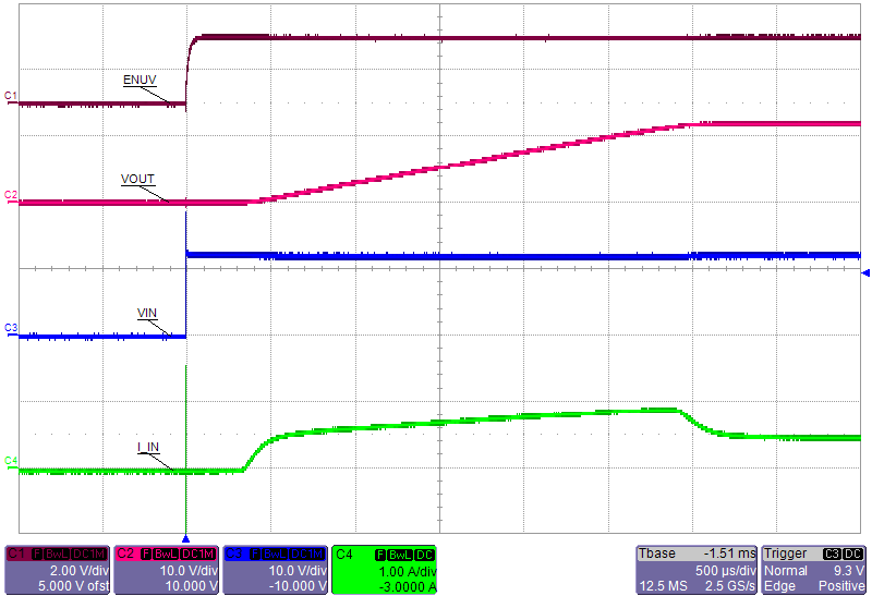
10.2.1.2.4 Setting Output Voltage Ramp time (tSS)
For a successful design, the junction temperature of device should be kept below the absolute-maximum rating during both dynamic (start-up) and steady state conditions. Dynamic power stresses often are an order of magnitude greater than the static stresses, so it is important to determine the right start-up time and in-rush current limit required with system capacitance to avoid thermal shutdown during start-up with and without load.
The ramp-up capacitor C(SS) needed is calculated considering the two possible cases:
10.2.1.2.4.1 Case1: Start-up Without Load: Only Output Capacitance C(OUT) Draws Current During Start-up
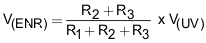
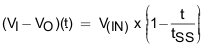
During start-up, as the output capacitor charges, the voltage difference across the internal FET decreases, and the power dissipated decreases as well. Typical ramp-up of output voltage V(OUT) with inrush current limit of 0.5A and power dissipated in the device during start-up is shown in Figure 31. The average power dissipated in the device during start-up is equal to area of triangular plot (red curve in Figure 32) averaged over tSS.
| V(IN) = 12 V | C(SS) = 1 nF | C(OUT)=100 µF |
| V(IN) = 12 V | C(SS) = 1 nF | C(OUT)=100 µF |
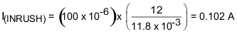
For TPS25921 device, the inrush current is determined as,
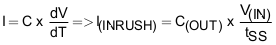
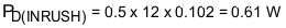
Power dissipation during start-up is:
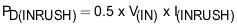
Equation 13 assumes that load does not draw any current until the output voltage has reached its final value.
10.2.1.2.4.2 Case 2: Start-up With Load: Output Capacitance C(OUT) and Load Draws Current During Start-up
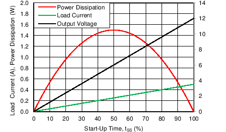
When load draws current during the turn-on sequence, there will be additional power dissipated. Considering a resistive load RL(SU) during start-up, load current ramps up proportionally with increase in output voltage during tSS time. Typical ramp-up of output voltage, load current and power dissipation in the device is shown in Figure 33 and power dissipation with respect to time is plotted in Figure 34. The additional power dissipation during start-up phase is calculated as follows.
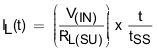
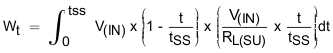
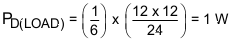
Where RL(SU) is the load resistance present during start-up. Average energy loss in the internal FET during charging time due to resistive load is given by:
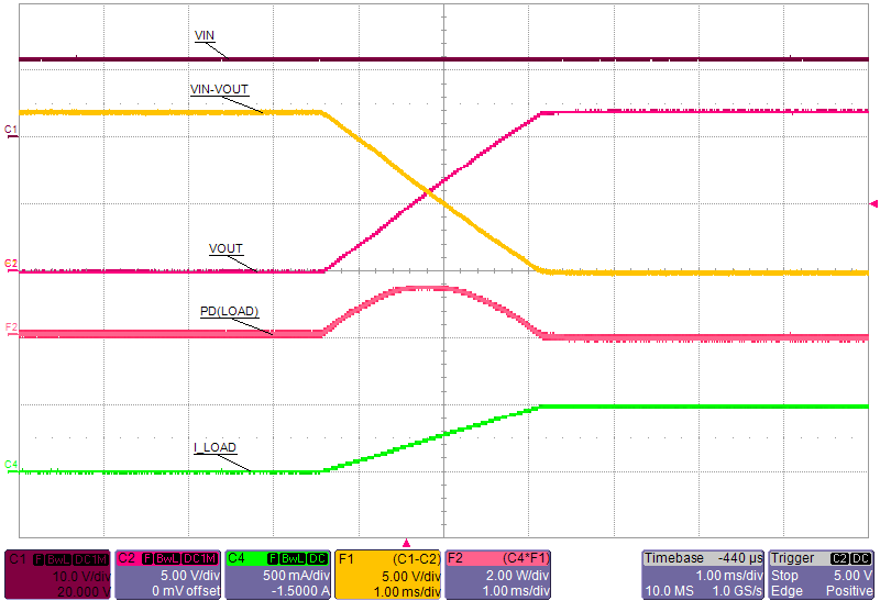
| V(IN) = 12 V | C(SS) = 1 nF , C(OUT)=100 µF | RL(SU) = 24 Ω |
| V(IN) = 12 V | C(SS) = 1 nF | RL(SU) = 24 Ω |
On solving Equation 16 the average power loss in the internal FET due to load is:
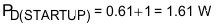
Total power dissipated in the device during startup is:

Total current during startup is given by:
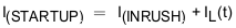
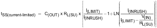
If I(STARTUP) > ILIMIT, the device limits the current to ILIMIT and the current limited charging time is determined by:
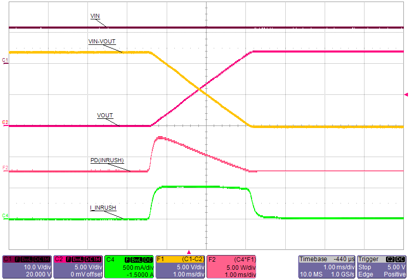
The power dissipation, with and without load, for selected start-up time should not exceed the shutdown limits as shown in Figure 35.
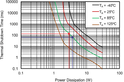 Figure 35. Thermal Shutdown Limit Plot
For the design example under discussion,
Select ramp-up capacitor C(SS) = 1nF, using Equation 2.
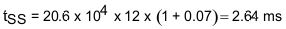
The inrush current drawn by the load capacitance (C(OUT)) during ramp-up using Equation 3.
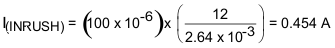
The inrush Power dissipation is calculated, using Equation 13.
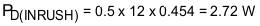
For 2.72 W of power loss, the thermal shut down time of the device should not be less than the ramp-up time tSS to avoid the false trip at maximum operating temperature. From thermal shutdown limit graph Figure 35 at
TA = 85°C, for 2.72 W of power the shutdown time is ~170 ms. So it is safe to use 2.64 ms as start-up time without any load on output.
Considering the start-up with load 24 Ω, the additional power dissipation, when load is present during start up is calculated, using Equation 17.
The total device power dissipation during start up is:
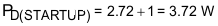
From thermal shutdown limit graph at TA = 85°C, the thermal shutdown time for 3.72 W is close to 60 ms. It is safe to have 30% margin to allow for variation of system parameters such as load, component tolerance, and input voltage. So it is well within acceptable limits to use the 1 nF capacitor with start-up load of 24 Ω.
If there is a need to decrease the power loss during start-up, it can be done with increase of C(SS) capacitor.
To illustrate, choose C(SS) = 4.7 nF as an option and recalculate:

From thermal shutdown limit graph at TA = 85°C, the shutdown time for 1.61 W power dissipation is ~1000 ms, which increases the margins further for shutdown time and ensures successful operation during start up and steady state conditions.
The spreadsheet tool available on the web can be used for iterative calculations.
10.2.1.2.5 Support Component Selections - R4 and CIN
Reference to application schematics, R4 is required only if FLT is used; The resistor serves as pull-up for the open-drain output driver. The current sunk by this pin should not exceed 100 mA (refer to the Absolute Maximum Ratings table). CIN is a bypass capacitor to help control transient voltages, unit emissions, and local supply noise. Where acceptable, a value in the range of 0.001 μF to 0.1 μF is recommended for C(IN).
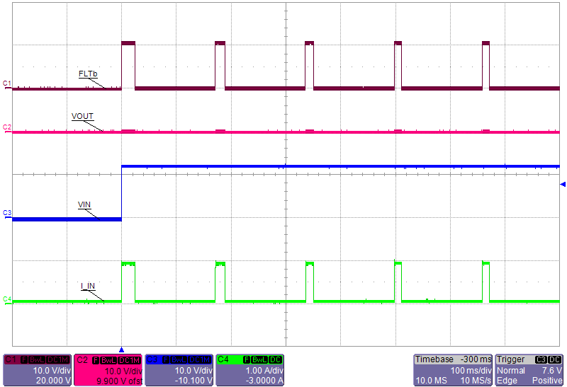
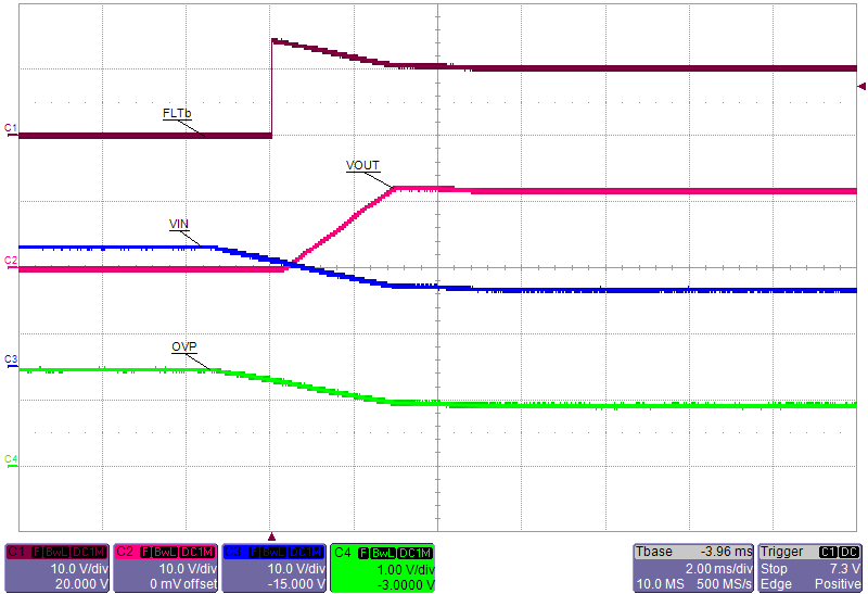
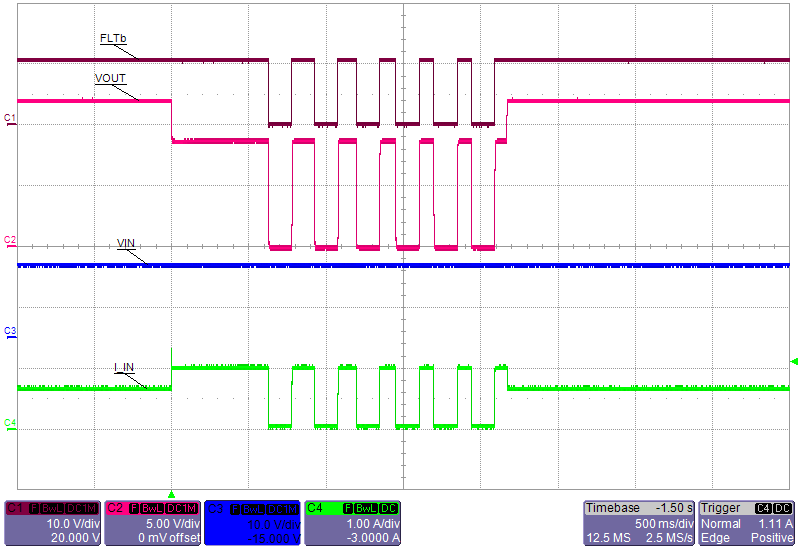
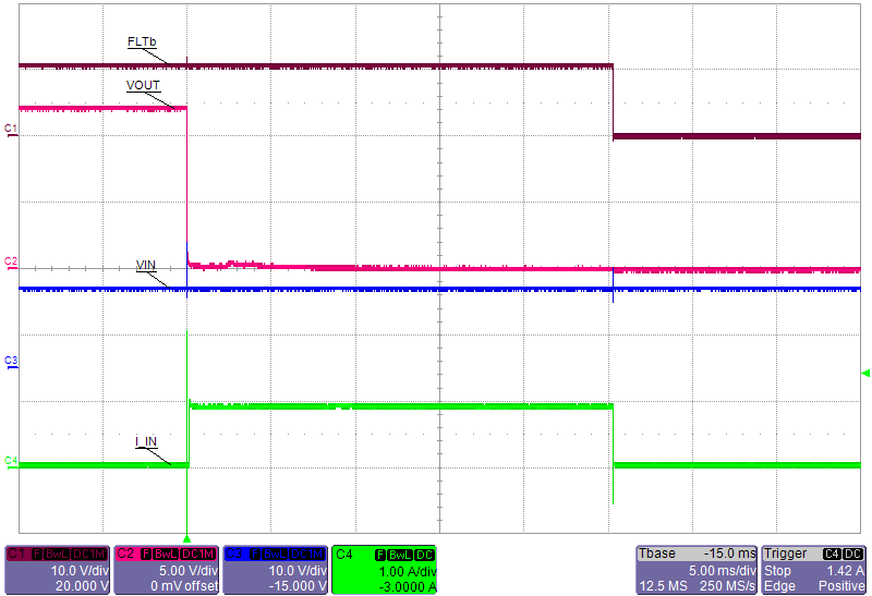
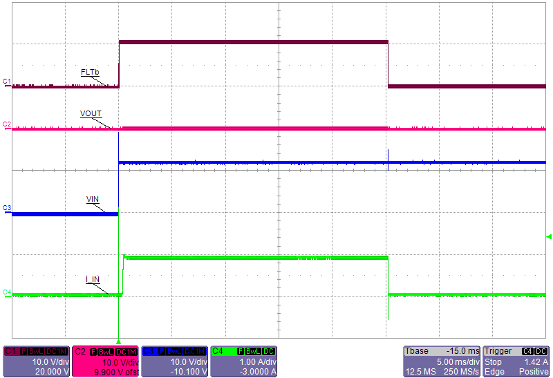
10.2.1.3 Application Curves