ZHCSCQ0 August 2014 TPS25921A , TPS25921L
PRODUCTION DATA.
- 1 特性
- 2 应用范围
- 3 说明
- 4 应用电路原理图
- 5 修订历史记录
- 6 Pin Configuration and Functions
- 7 Specifications
- 8 Parametric Measurement Information
-
9 Detailed Description
- 9.1 Overview
- 9.2 Functional Block Diagram
- 9.3 Feature Description
- 9.4 Device Functional Modes
-
10Applications and Implementation
- 10.1 Application Information
- 10.2
Typical Application
- 10.2.1
Precision Current Limiting and Protection for White Goods
- 10.2.1.1 Design Requirements
- 10.2.1.2 Detailed Design Procedure
- 10.2.1.3 Application Curves
- 10.2.1
Precision Current Limiting and Protection for White Goods
- 11System Examples
- 12Power Supply Recommendations
- 13Layout
- 14器件和文档支持
- 15机械封装和可订购信息
1 特性
- 4.5V - 18V 工作电压,最大绝对值 20V
- 90mΩ RDS(ON)(典型值)
- 0.4A 至 1.6A 可调电流限值
- ILIMIT 为 1A 且温度为 25°C 时限流精度达 ±2%
- ±3% 过压、欠压阈值
- 可编程的 dVO/dt 控制
- 热关断故障输出、欠压闭锁 (UVLO) 和过压保护 (OVP)
- -40°C 至 125°C 的结温范围
- 自动重试和闭锁型号
- UL2367 认证正在处理中
- UL60950 - 单点故障测试期间安全
2 应用范围
- 大型家用电器,家用电器
- 机顶盒、数字化视频光盘 (DVD) 和游戏机
- 硬盘 (HDD) 和固态硬盘 (SSD)
- 智能仪表,气体分析仪
- 智能负载开关
- USB 开关
- 电源适配器器件
3 说明
TPS25921 是一款具有全套保护功能的紧凑型多功能熔丝。 它具有较宽的工作电压,可实现对多种常用直流 (DC) 总线的控制。 室温下限流精度达 ±2%,这种优异的精度使得 TPS25921 成为多种系统保护应用的理想选择。
而且它还具有过流保护、过压保护和欠压保护等多种可编程功能,能够对负载、电源和器件提供保护。欠压和过压条件下的阈值精度为 3%,无需监控电路即可确保对总线电压进行严密控制。 此外,还针对系统状态监视和下游负载控制提供了故障标志输出 (FLT)。
对于热插拔电路板,TPS25921 提供了浪涌电流控制和可编程的输出斜坡速率。 为实现设计灵活性的最大化,可使用软启动 (SS) 引脚处的电容器编程设定输出斜坡速率。
器件信息(1)
| 部件号 | 封装 | 封装尺寸(标称值) |
|---|---|---|
| TPS25921A | SOIC | 4.90mm x 3.91mm |
| TPS25921L |
- 如需了解所有可用封装,请见数据表末尾的可订购产品附录。
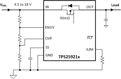
4 应用电路原理图
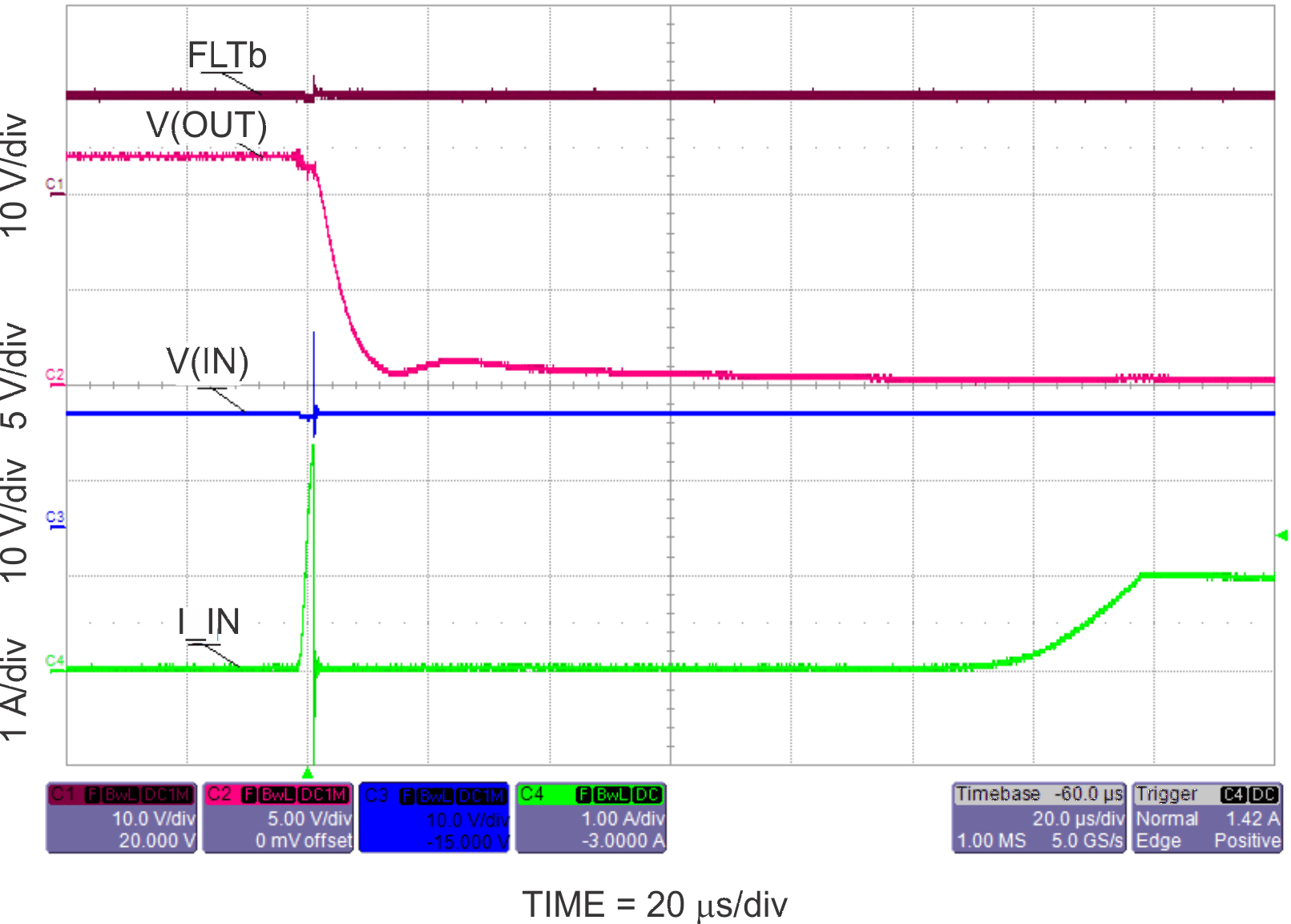
12V 短路响应