ZHCSDK8 March 2015 TPS24770 , TPS24771 , TPS24772
PRODUCTION DATA.
- 1 特性
- 2 应用
- 3 说明
- 4 简化电路原理图
- 5 修订历史记录
- 6 Device Comparison Table
- 7 Pin Configuration and Functions
- 8 Specifications
-
9 Detailed Description
- 9.1 Overview
- 9.2 Functional Block Diagram
- 9.3
Feature Description
- 9.3.1 Enable and Over-voltage Protection
- 9.3.2 Current Limit and Power Limit during Start-up
- 9.3.3 Two Level Protection During Regular Operation
- 9.3.4 Dual Timer (TFLT and TINR)
- 9.3.5 3 Options for Response to a Fast Trip
- 9.3.6 Using Soft Start - IHGATE and TINR Considerations
- 9.3.7 Analog Current Monitor
- 9.3.8 Power Good Flag
- 9.3.9 Fault Reporting
- 9.4 Device Functional Modes
-
10Application and Implementation
- 10.1 Application Information
- 10.2
Typical Application
- 10.2.1 12 V, 100 A, 5,500 µF Analog Hot Swap Design
- 10.2.2 Design Requirements
- 10.2.3
Detailed Design Procedure
- 10.2.3.1 Select RSNS and VSNS,CL Setting
- 10.2.3.2 Selecting the Fast Trip Threshold and Filtering
- 10.2.3.3 Selecting the Hot Swap FET(s)
- 10.2.3.4 Select Power Limit
- 10.2.3.5 Set Fault Timer
- 10.2.3.6 Check MOSFET SOA
- 10.2.3.7 Choose Under Voltage and Over Voltage Settings
- 10.2.3.8 Selecting C1 and COUT
- 10.2.3.9 Adding CENHS
- 10.2.3.10 Selecting D1 and D2
- 10.2.3.11 Checking Stability
- 10.2.3.12 Compute Tolerances
- 10.2.4 Application Curves
- 10.2.5
240 VA Application Using CSD16415Q5B
- 10.2.5.1 Design Requirements
- 10.2.5.2 Theory of Operations
- 10.2.5.3
Design Procedure
- 10.2.5.3.1
Select VSNS,CL, RSNS, and RSET Setting
- 10.2.5.3.1.1 Select RPOW and RIMON
- 10.2.5.3.1.2 Selecting the Hot Swap FET(s)
- 10.2.5.3.1.3 Keeping MOSFET within SOA During Normal Start-up
- 10.2.5.3.1.4 Choose Fault Timer
- 10.2.5.3.1.5 Choose Under Voltage and Over Voltage Settings
- 10.2.5.3.1.6 Selecting CIN and COUT
- 10.2.5.3.1.7 Selecting D1 and D2
- 10.2.5.3.1.8 Adding CENHS
- 10.2.5.3.1.9 Stability Considerations
- 10.2.5.3.1
Select VSNS,CL, RSNS, and RSET Setting
- 10.2.5.4 Application Curves
- 10.2.6 240 VA Application Using CSD17573Q5B
- 11Power Supply Recommendations
- 12Layout
- 13器件和文档支持
- 14机械、封装和可订购信息
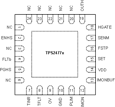
7 Pin Configuration and Functions
QFN 24-Pin with Thermal Pad
RGE Package
Top View

Pin Functions
| PIN | TYPE(1) | DESCRIPTION | |
|---|---|---|---|
| NAME | NO. | ||
| ENHS | 2 | I | Active-high enable input of Hot Swap. Logic input. Connects to resistor divider. |
| FLTb | 4 | O | Active-low, open-drain output indicating various faults. |
| FSTP | 16 | I | Fast trip programming set pin for Hot Swap. A resistor is connected from positive terminal of RSNS to FSTP. |
| GND | 10 | – | Ground. |
| HGATE | 18 | O | Gate driver output for external Hot Swap MOSFET. |
| IMON | 12 | I/O | Analog monitor and current limit program point. Connect RIMON to ground. |
| IMONBUF | 13 | O | Voltage output proportional to the load current (0V–3.0V). |
| NC | 1,3, 6, 20–24 | NC | No connect. Tie to ground or leave floating. |
| OUTH | 19 | I | Output voltage sensor for monitoring Hot Swap MOSFET's power. Connects to the source terminal of the Hot Swap N channel MOSFET. |
| OV | 9 | I | Overvoltage comparator input. Connects to resistor divider. HGATE is pulled low when OV exceeds the threshold. Connect to ground when not used. |
| PGHS | 5 | O | Active-high, open-drain power-good indicator. |
| PLIM | 11 | I | Power limit programming pin. A resistor from this pin to GND sets the maximum power dissipation for the Hot Swap FET. Connect a 4.99 kΩ resistor to disable power limit. |
| SENM | 17 | I | Current-sensing input for the sense resistor. Directly connects to the negative terminal of the sense resistor. |
| SET | 15 | I | Current-limit programming set pin for Hot Swap. A resistor is connected from positive terminal of the sensing resistor. |
| TFLT | 8 | I/O | Fault timer, which runs when the device is in regular operation and there is an overcurrent condition. |
| TINR | 7 | I/O | Inrush timer, which runs during the inrush operation (start-up) if the part is in current limit or power limit. |
| VDD | 14 | P | Power Supply |
(1) I = Input; O = Output ; P = Power, NC = No Connect