ZHCSGK9B April   2017  – December 2017 TPS22971

PRODUCTION DATA.  

  1. 特性
  2. 应用
  3. 说明
    1.     Device Images
      1.      典型应用
  4. 修订历史记录
  5. Pin Configuration and Functions
    1.     Pin Functions
  6. Specifications
    1. 6.1 Absolute Maximum Ratings
    2. 6.2 ESD Ratings
    3. 6.3 Recommended Operating Conditions
    4. 6.4 Thermal Information
    5. 6.5 Electrical Characteristics
    6. 6.6 Switching Characteristics
    7. 6.7 Typical DC Characteristics
    8. 6.8 Typical AC Characteristics
  7. Parameter Measurement Information
  8. Detailed Description
    1. 8.1 Overview
    2. 8.2 Functional Block Diagram
    3. 8.3 Feature Description
      1. 8.3.1 On and Off Control
      2. 8.3.2 Controlled Turn-On
      3. 8.3.3 Power Good (PG)
      4. 8.3.4 Quick Output Discharge (QOD)
    4. 8.4 Device Functional Modes
  9. Application and Implementation
    1. 9.1 Application Information
      1. 9.1.1 Thermal Consideration
      2. 9.1.2 PG Pull Up Resistor
      3. 9.1.3 Power Sequencing
    2. 9.2 Typical Application
      1. 9.2.1 Design Requirements
      2. 9.2.2 Detailed Design Procedure
        1. 9.2.2.1 Maximum Voltage Drop and On-Resistance
        2. 9.2.2.2 Managing Inrush Current
      3. 9.2.3 Application Curves
  10. 10Power Supply Recommendations
  11. 11Layout
    1. 11.1 Layout Guidelines
    2. 11.2 Layout Example
  12. 12器件和文档支持
    1. 12.1 文档支持
      1. 12.1.1 相关文档
    2. 12.2 接收文档更新通知
    3. 12.3 社区资源
    4. 12.4 商标
    5. 12.5 静电放电警告
    6. 12.6 Glossary
  13. 13机械、封装和可订购信息

封装选项

机械数据 (封装 | 引脚)
散热焊盘机械数据 (封装 | 引脚)
订购信息

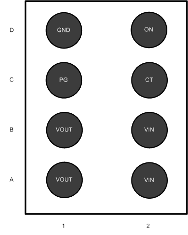
Pin Configuration and Functions

YZP Package
8-Pin DSBGA
Laser Marking View
TPS22971 PIN-Configuration-1.gif
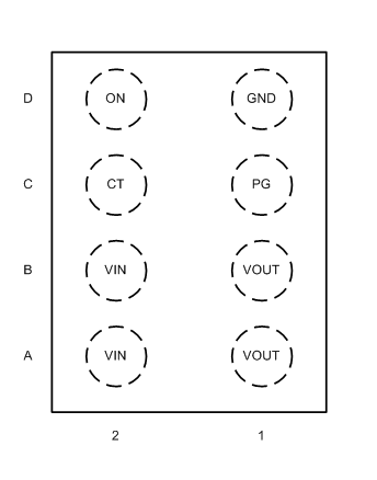
YZP Package
8-Pin DSBGA
Bump View
TPS22971 TPS22971_Pinout.gif

Pin Functions

PINI/ODESCRIPTION
NAMENO.
CT C2 O VOUT slew rate control. Adding capacitance from this pin to ground lowers the output slew rate
GND D1 GND Ground
ON D2 I Switch enable control input. Do not leave floating
PG C1 O Power Good Indication. Open drain releases when the switch is fully on
VOUT A1, B1 O Switch output
VIN A2, B2 I Switch input