ZHCSFR6C December 2016 – January 2018 TPS22810
PRODUCTION DATA.
- 1 特性
- 2 应用
- 3 说明
- 4 修订历史记录
- 5 Device Comparison Table
- 6 Pin Configuration and Functions
- 7 Specifications
- 8 Parameter Measurement Information
- 9 Detailed Description
- 10Application and Implementation
- 11Power Supply Recommendations
- 12Layout
- 13器件和文档支持
- 14机械、封装和可订购信息
封装选项
机械数据 (封装 | 引脚)
散热焊盘机械数据 (封装 | 引脚)
- DRV|6
订购信息
10.5.2.1 Shutdown Sequencing During Unexpected Power Loss
Using the adjustable Quick Output Discharge function of the TPS22810, adding a load switch to each power rail can be used to manage the power down sequencing in the event of an unexpected power loss (that is battery removal). To determine the QOD values for each load switch, first confirm the power down order of the device you wish to power sequence. Be sure to check if there are voltage or timing margins that must be maintained during power down. Next, consult Table 1 to determine appropriate CL and RQOD values for each power rail's load switch so that the load switches' fall times correspond to the order in which they need to be powered down. In the above example, we must have this power rail's fall time to be 4 ms. Using Equation 2, we can determine the appropriate RQOD to achieve our desired fall time.
Since fall times are measured from 90% of VOUT to 10% of VOUT, using Equation 2, we get Equation 4 and Equation 5.

Consulting Figure 6, RPD at VIN = 12 V is approximately 250 Ω. Using Equation 1, the required external QOD resistance can be calculated as shown in Equation 6 and Equation 7.
Figure 22 through Figure 25 are scope shots demonstrating an example of the QOD functionality when power is removed from the device (both ON and VIN are disconnected simultaneously). In the scope shots, the VIN = 12 V and correspond to when RQOD = 1000 Ω, RQOD= 500 Ω, and QOD = VOUT with two values of CL = 10 µF and 22 µF.
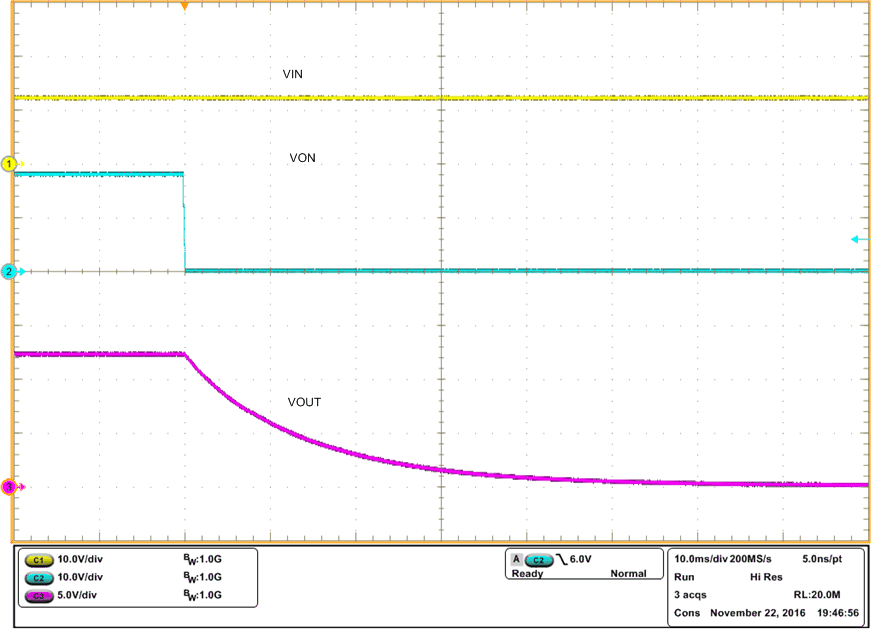
| VIN = 12 V | CIN = 1 µF | CL = 10 µF |
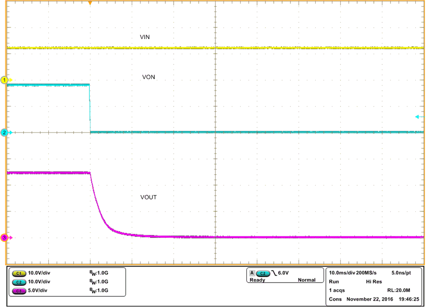
| VIN = 12 V | CIN = 1 µF | CL = 10 µF |
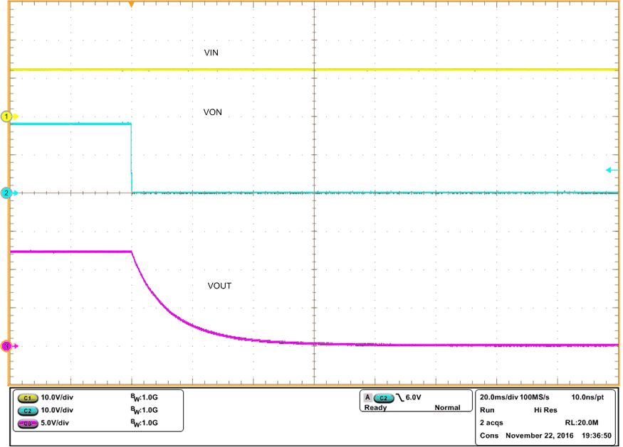
| VIN = 12 V | CIN = 1 µF | CL = 22 µF |
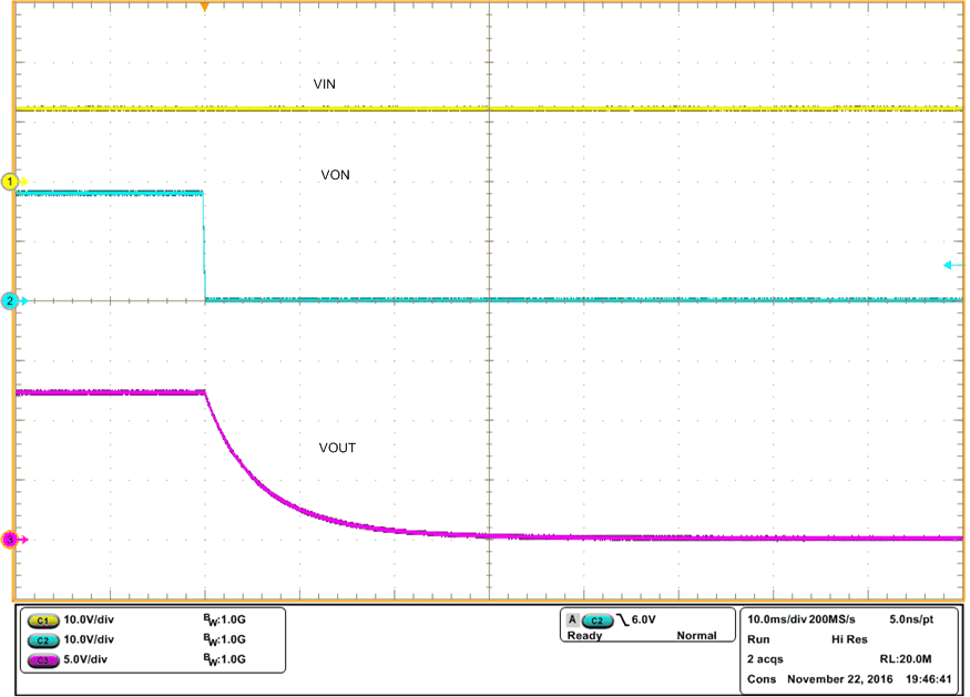
| VIN = 12 V | CIN = 1 µF | CL = 10 µF |
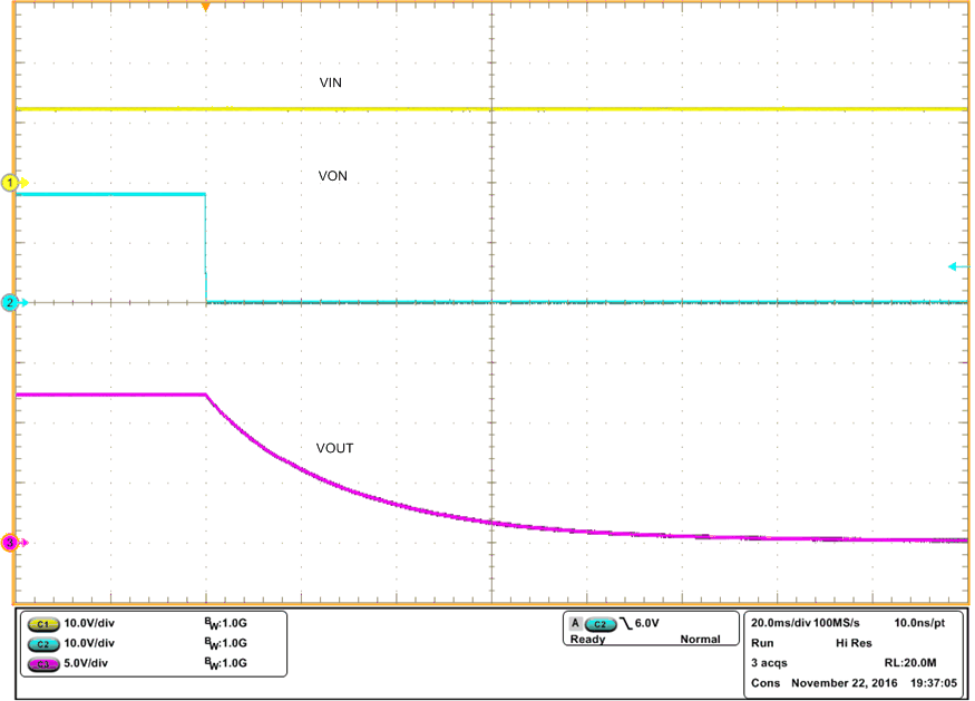
| VIN = 12 V | CIN = 1 µF | CL = 22 µF |
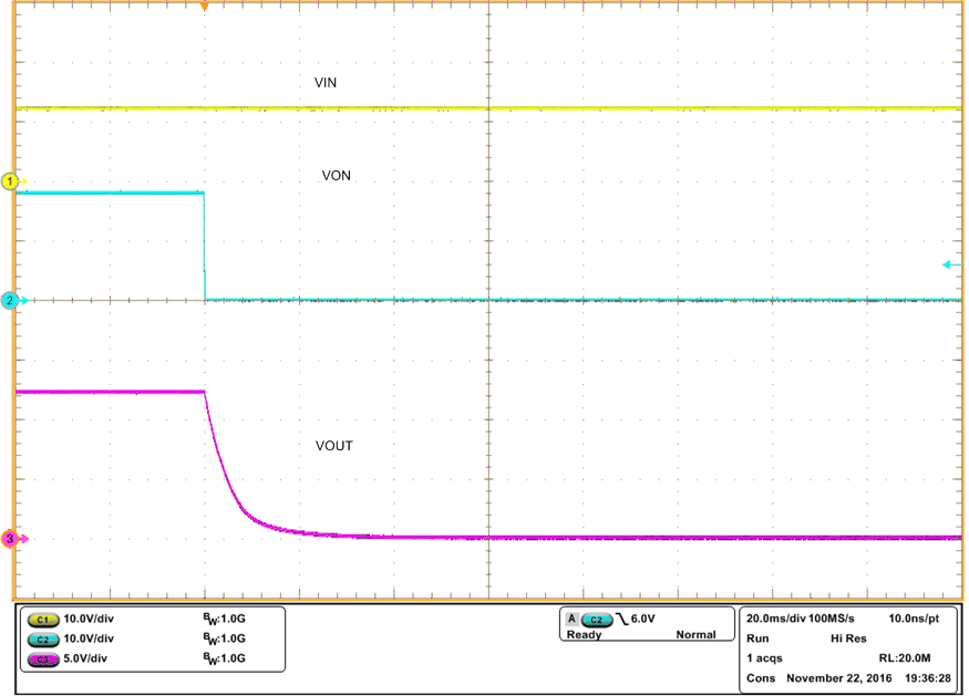
| VIN = 12 V | CIN = 1 µF | CL = 22 µF |