SLVSAX6H October 2011 – December 2015 TPS2002C , TPS2003C , TPS2052C , TPS2060C , TPS2062C , TPS2062C-2 , TPS2064C , TPS2064C-2 , TPS2066C , TPS2066C-2
PRODUCTION DATA.
- 1 Features
- 2 Applications
- 3 Description
- 4 Revision History
- 5 Device Comparison Table
- 6 Pin Configuration and Functions
- 7 Specifications
- 8 Parameter Measurement Information
- 9 Detailed Description
- 10Application and Implementation
- 11Power Supply Recommendations
- 12Layout
- 13Device and Documentation Support
- 14Mechanical, Packaging, and Orderable Information
6 Pin Configuration and Functions
DGN Package
8-Pin MSOP
Top View

D Package
8-Pin SOIC
Top View

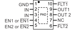
DRC Package
10-Pin VSON
Top View

DRB Package
8-Pin SON
Top View

Pin Functions
| PIN | TYPE(3) | DESCRIPTION | ||||
|---|---|---|---|---|---|---|
| NAME | MSOP | SOIC | VSON | SON | ||
| GND | 1 | 1 | 1 | 1 | GND | Ground connection |
| IN | 2 | 2 | 2, 3 | 2 | I | Input voltage and power-switch drain; connect a 0.1 µF or greater ceramic capacitor from IN to GND close to the IC |
| EN1 | 3(1) | 3(6) | 4(4) | — | I | Enable input channel 1, logic high turns on power switch |
| –(2) | –(7) | –(5) | — | |||
| EN1 | –(1) | –(6) | –(4) | 3 | I | Enable input channel 1, logic low turns on power switch |
| 3(2) | 3(7) | 4(5) | ||||
| EN2 | 4(1) | 4(6) | 5(4) | — | I | Enable input channel 2, logic high turns on power switch |
| –(2) | –(7) | –(5) | — | |||
| EN2 | –(1) | –(6) | –(4) | 4 | I | Enable input channel 2, logic low turns on power switch |
| 4(2) | 4(7) | 5(5) | ||||
| FLT2 | 5 | 5 | 6 | 5 | O | Active-low open-drain output, asserted during overcurrent, or overtemperature conditions on channel 2 |
| NC | — | — | 7 | — | O | No connect – leave floating |
| OUT2 | 6 | 6 | 8 | 6 | O | Power-switch output channel 2, connected to load |
| OUT1 | 7 | 7 | 9 | 7 | O | Power-switch output channel 1, connected to load |
| FLT1 | 8 | 8 | 10 | 8 | O | Active-low open-drain output, asserted during over-current, or overtemperature conditions on channel 1 |
| PowerPAD™ | PAD | — | PAD | — | GND | Internally connected to GND; used to heat-sink the part to the circuit board traces. Connect PAD to GND plane as a heatsink. |
(1) Applies to TPS2052C, TPS2066C, TPS2066C-2, TPS2064C, and TPS2064C-2
(2) Applies to TPS2062C and TPS2060C
(3) I = Input, O = Output, GND = Ground
(4) Applies to TPS2003C
(5) Applies to TPS2002C
(6) Applies to TPS2066C
(7) Applies to TPS2062C