ZHCSEQ4 July 2015 TPIC2060A
PRODUCTION DATA.
- 1 特性
- 2 应用
- 3 说明
- 4 修订历史记录
- 5 说明 (续)
- 6 Pin Configuration and Functions
- 7 Specifications
-
8 Detailed Description
- 8.1 Overview
- 8.2 Functional Block Diagram
- 8.3 Feature Description
- 8.4 Device Functional Modes
- 8.5 Programming
- 8.6
Register Maps
- 8.6.1 Register State Transition
- 8.6.2 DAC Register (12-Bit Write Only)
- 8.6.3 Control Register (8-Bit Read/Write)
- 8.6.4
Detailed Register Description
- 8.6.4.1 REG01 12-Bit DAC for Tilt (offset = 01h)
- 8.6.4.2 REG02 12-Bit DAC for Focus (offset = 02h)
- 8.6.4.3 REG03 12-Bit DAC for Tracking (offset = 03h)
- 8.6.4.4 REG04 12-Bit DAC for Sled1 (offset = 04h)
- 8.6.4.5 REG05 12-Bit DAC for Sled2 (offset = 05h)
- 8.6.4.6 REG06 12-Bit DAC for Stepping1 (offset = 06h)
- 8.6.4.7 REG07 12-Bit DAC for Stepping2 (offset = 07h)
- 8.6.4.8 REG08 12-Bit DAC for Spindle (offset = 08h)
- 8.6.4.9 REG09 12-Bit DAC for Load (offset = 09h)
- 8.6.4.10 REG70 8-Bit Control Register for DriverEna (offset = 70h)
- 8.6.4.11 REG71 8-Bit Control Register for FuncEna (offset = 71h)
- 8.6.4.12 REG72 8-Bit Control Register for ACTCfg (offset = 72h)
- 8.6.4.13 REG73 8-Bit Control Register for Parm0 (offset = 73h)
- 8.6.4.14 REG74 8-Bit Control Register for SIFCfg (offset = 74h)
- 8.6.4.15 REG75 8-Bit Control Register for Parm1 (offset = 75h)
- 8.6.4.16 REG76 8-Bit Control Register for WriteEna (offset = 76h)
- 8.6.4.17 REG77 8-Bit Control Register for ClrReg (offset = 77h)
- 8.6.4.18 REG78 8-Bit Control Register for ActTemp (offset = 78h)
- 8.6.4.19 REG79 8-Bit Control Register for UVLOMon (offset = 79h)
- 8.6.4.20 REG7A 8-Bit Control Register for TSDMon (offset = 7Ah)
- 8.6.4.21 REG7B 8-Bit Control Register for SCPMon (offset = 7Bh)
- 8.6.4.22 REG7C 8-Bit Control Register for TempMon (offset = 7Ch)
- 8.6.4.23 REG7D 8-Bit Control Register for Status Monitor (offset = 7Dh)
- 8.6.4.24 REG7E 8-Bit Control Register for Version (offset = 7Eh)
- 8.6.4.25 REG7F 8-Bit Control Register for Status (offset = 7Fh)
- 8.6.4.26 REG60 8-Bit Control Register for SPMCfg (offset = 60h)
- 8.6.4.27 REG61 8-Bit Control Register for SPMCfg (offset = 61h)
- 8.6.4.28 REG62 8-Bit Control Register for SPMCfg (offset = 62h)
- 8.6.4.29 REG64 8-Bit Control Register for Protect (offset = 64h)
- 8.6.4.30 REG65 8-Bit Control Register for SPMCfg (offset = 65h)
- 8.6.4.31 REG68 8-Bit Control Register for Protect (offset = 68h)
- 8.6.4.32 REG6B 8-Bit Control Register for DisProt (offset = 6Bh)
- 8.6.4.33 REG6C 8-Bit Control Register for ENDCfg (offset = 6Ch)
- 8.6.4.34 REG6E 8-Bit Control Register for UtilCfg (offset = 6Eh)
- 8.6.4.35 REG6F 8-Bit Control Register for GPOUTSet (offset = 6Fh)
-
9 Application and Implementation
- 9.1
Application Information
- 9.1.1 DAC Type
- 9.1.2 Example of 12-Bit DAC Sampling Rate for FCS/TRK/TLT
- 9.1.3 Digital Input Coding
- 9.1.4 Example Timing of Target Control System
- 9.1.5 Spindle Motor Driver Operating Sequence
- 9.1.6 Auto Short Brake Function
- 9.1.7 Spindle PWM Control
- 9.1.8 Spindle Driver Current Limit Circuit
- 9.1.9 Sled Driver Part
- 9.1.10 Stepping Driver Part
- 9.1.11 Focus/Track/Tilt Driver Part
- 9.1.12 Load Driver Part
- 9.1.13 End Detect Function
- 9.1.14 Load Tray Lock Detect Function
- 9.1.15 Load Tray Push Detect Function
- 9.1.16 Monitor Signal on GPOUT
- 9.1.17 9-V LDO
- 9.2 Typical Application
- 9.1
Application Information
- 10Power Supply Recommendations
- 11Layout
- 12器件和文档支持
- 13机械、封装和可订购信息
9 Application and Implementation
NOTE
Information in the following applications sections is not part of the TI component specification, and TI does not warrant its accuracy or completeness. TI’s customers are responsible for determining suitability of components for their purposes. Customers should validate and test their design implementation to confirm system functionality.
9.1 Application Information
9.1.1 DAC Type
The TPIC2060A has nine-channel drivers and each channel is assigned to the most suitable DAC engine with a different type. ACT (FCS/TRK/TLT) has a 12-bit DAC. The upper 8 (MSB sign bit) are sampled in 5 MHz, and LSB 4 bits are output in sequence with 1.25-MHz PWM. SPIN and load DAC have the same types and sampling rate with 312 kHz. The SPM channel has 14× gain, and other channels (except SLED and STP) have 6× gain. The DAC for STP is 8-bit resolution output with 40-kHz PWM, and no feedback. The gain for STP is 5× relative to P5V voltage. Table 42 shows the configuration of each driver.
Table 42. DAC Type
| FCS/TRK/TLT | SLED | SPIN | LOAD | STP | |
|---|---|---|---|---|---|
| Resolution | 12 bit | 10 bit | 12 bit | 12 bit | 8 bit |
| Type | 8-bit oversampling | 10-bit voltage DAC | 8-bit oversampling | 8-bit oversampling | 1-bit direct duty PWM |
| Sampling | 1.25M / 10 bit 312K / 12 bit |
312K | 312K | 40 kHz | |
| PWM frequency | 312 kHz | About 156 kHz (variable) | 156 kHz | 312 kHz | 40 kHz |
| Out range | ±6 V | ±880 mA | ±14 V | ±6V | ±(P5V*1) |
| Feedback | Voltage F/B | Current F/B | Power supply compensation | Voltage F/B shared with TRK | Direct PWM No F/B |
9.1.2 Example of 12-Bit DAC Sampling Rate for FCS/TRK/TLT
The input data is separated in the upper 8 bits and the lower 4 bits. Upper 8 bits (MSB sign 1 bit) are put into 8-bit current DAC in every 5 MHz. The lower 4 bits are put into one bit current DAC in sequence from upper to lower bit. This is a one-bit DAC output with PWM in 1.25 MHz. Any PWM duty, 100%, 75%, 50%, 25%, or 0%, is summed in 8-bit current DAC every 1.25 MHz. Thus, it takes 3.2 µs for all lower 4 bits summing to the PWM output. As a result, 12-bit data is sampled in every PWM cycle. Figure 49 shows an example of the sampling rate for FCS/TRK/TLT.
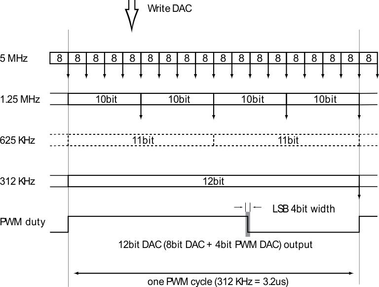 Figure 49. Example of 12-Bit DAC Conversion Time (FCS/TRK/TLT)
9.1.3 Digital Input Coding
The output voltage (current) is commanded through programming to the DAC. All of the DAC input format is 12 bit in complements of 2's, though some DAC has a low resolution. When 12 bits of data is input as 8-bits DAC, the TPIC2060A recognizes four subordinate position bits (LSB) as 0. To arrange for 12-bit DAC format, DSP should shift 8-bit or 10-bit data to an appropriate bit position. The full scale is ±1.0 V and driver gain is set to 6 or 14. The output voltage (Vout) is given by the following equation:
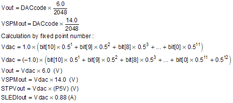
where
Table 43. DAC Format
| MSB Digital input (BIN) LSB | Hex | Dec | Vdac | Analog Output (5 V) | Analog Output (12 V) |
|---|---|---|---|---|---|
| 1000_0000_0000 | 0x800 | –2048 | –0.9995 | –5.997 | –13.993 |
| 1000_0000_0001 | 0x801 | –2047 | –0.9995 | –5.997 | –13.993 |
| 1111_1111_1111 | 0xFFF | –1 | –0.0005 | –0.003 | –0.007 |
| 0000_0000_0000 | 0x000 | 0 | 0 | 0.000 | 0.000 |
| 0000_0000_0001 | 0x001 | 1 | 0.0005 | 0.003 | 0.007 |
| 0111_1111_1110 | 0x7FE | 2046 | 0.9990 | 5.994 | 13.986 |
| 0111_1111_1111 | 0x7FF | 2047 | 0.9995 | 5.997 | 13.993 |
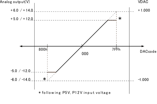 Figure 50. Output Voltage vs DAC Code
9.1.4 Example Timing of Target Control System
The TPIC2060A is designed to meet the requirements for updating control data in 400 kHz. Table 44 lists an example of a control system parameter. It takes 0.51 µs to transmit a 16-bit data packet to the TPIC2060A with a 35-MHz SCLK. Therefore, DSP can be sent four packets at 400-kHz intervals. If the SCLK is lower than 28.8 MHz, the user must reduce packet quantity to less than three. For example, the Focus/Truck command updates every 2.5 µs (400 kHz), and can send another two kinds of packets during this time. Figure 51 shows an example of the control timing when using the TPIC2060A.
Table 44. Example Timing of Target Control System
| SIGNAL | BIT | UPDATE CYCLE (kHz) |
|---|---|---|
| Focus | 12 | 400 |
| Track | 12 | 400 |
| Tilt | 12 | 100 |
| Sled1 | 10 | 100 |
| Sled2 | 10 | 100 |
| Spindle | 12 | 100 |
| Load | 12 | — |
| Step1 | 8 | 40 |
| Step2 | 8 | 40 |
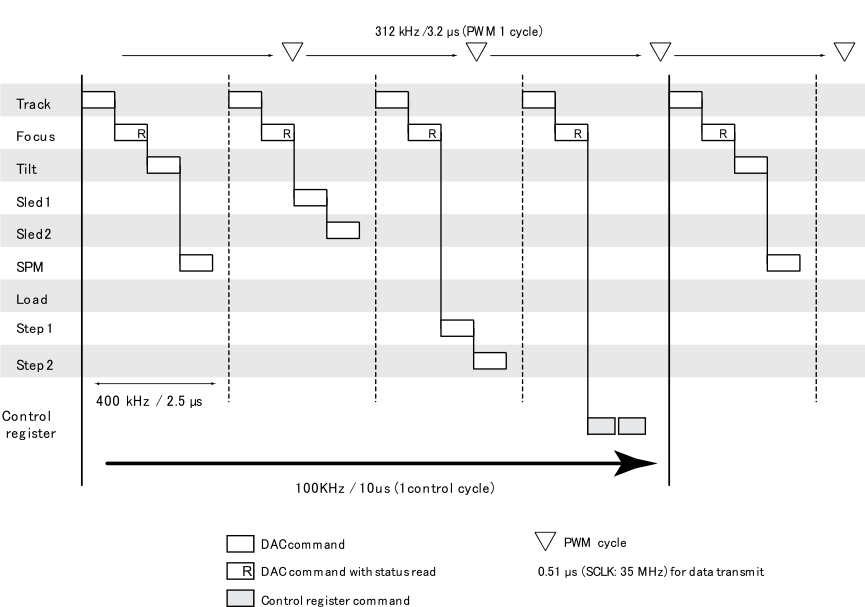 Figure 51. Example DAC Control
9.1.5 Spindle Motor Driver Operating Sequence
When the VSPM is set to a positive DAC code, it goes into acceleration mode. Initial position sense (IS) mode then operates, the start-up circuits offer a start-up pattern sequence to the driver, and then switch to spin-up mode by detecting the rotor position through BEMF signal from the spindle motor coil.
The spin-down and brake functions are also controlled by the DAC value, VSPM. When the brake command to VSPM is set, the driver goes into active-brake mode, switches to short-brake mode in slow revolution speed, and then stops automatically. The FG signal is composed from EXOR of a three-phase signal and is output from XFG pin shown in Figure 52.
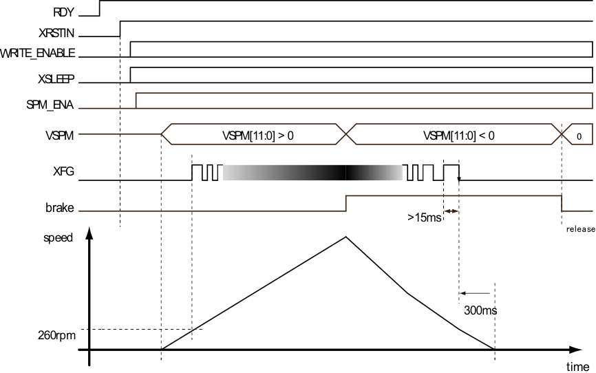 Figure 52. Spindle Operating Sequence
Use the down-edge of the FG signal for monitoring the FG frequency.
Short brake mode is asserted after 300 ms of FG signal stays L-level in deceleration.
This value is the nominal number of using a 12-pole motor.
9.1.6 Auto Short Brake Function
The TPIC2060A provides an auto short brake function that selects the brake mode automatically by motor speed. The auto short brake is an intelligent brake function that includes two modes, short brake and active brake. If a value of 0xF90 or less is set to VSPM, brake mode automatically changes at rotation speed. This function enables low-power consumption and silent braking. Table 45 shows the relation between brake mode and speed. The overspeed protection function suspends the SPM driver output at 15000 or more revolutions.
Table 45. Brake Mode
| VSPM[11:0] | MODE | ROTATION SPEED (RPM)(1) | |||
|---|---|---|---|---|---|
| ABOUT 11500 | ABOUT 11500 TO 5600 | ABOUT 5600 TO 4000 | ABOUT 4000 TO 0 | ||
| 0x000 - 0xFDD | Manual | 2-phase short brake | |||
| 0xFDC - 0xF90 | Manual | Active brake | |||
| 0xF8F - 0xADB | Auto short | Free run | 3-phase short brake(2) | Active brake | |
| 0xADA - 0x800 | Auto short | Free run | 3-phase short brake(3) | Active brake | |
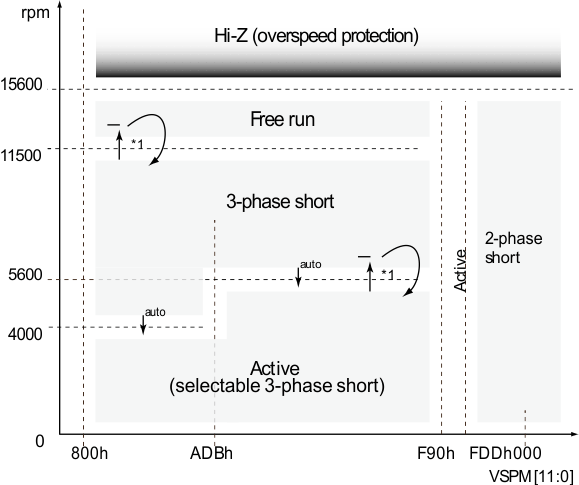
9.1.7 Spindle PWM Control
The output PWM duty of the spindle is controlled by DAC code (VSPM). The gain in acceleration setting is always 14 times, while the maximum output is restricted to P12V voltage. A dead band which outputs = 0 exists in the width of plus or minus 0x52, focusing on zero.
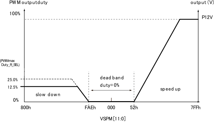 Figure 54. Spindle PWM Control
9.1.8 Spindle Driver Current Limit Circuit
This IC builds in the SPM current sense resistor, which can select the resistor value. The spindle current limit circuit monitors motor current (which flows through this resistance) and limits the output current by reducing PWM duty when detecting overcurrent conditions. Table 46 shows resistor value. A limit current value can be calculated from following formula, where the resistor value is the equivalent resistance for a current limit calculation:
Table 46. SPM Current Sense Resistor
| SPM_RCOM_SEL[1:0] | RESISTANCE VALUE (Ω)(1) | LIMIT CURRENT (mA) |
|---|---|---|
| 00 | 0.15 | 1133 |
| 01 | 0.22 | 772 |
| 10 | 0.12 | 1416 |
| 11 | 0.10 | 1700 |
9.1.9 Sled Driver Part
The sled driver outputs the PWM pulse set as DAC code (VSLDx) with current feedback. The maximum output is restricted to 880 mA at 0x7FF and 0x800. A dead band with output = 0 exists in the width of plus or minus 0x1F focusing on zero.
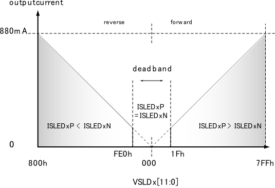 Figure 55. Sled Output Current
Both outputs of SLED1/2 are 'L' when the input code is in the dead band.
9.1.10 Stepping Driver Part
The step driver outputs the PWM pulse set as 8-bit DAC code (VSTPx) using VSTP[11:4]. There is no feedback monitor for output. The pulse duration according to the P5V power supply voltage is outputted.
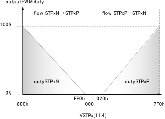 Figure 56. Step Output Duty
9.1.11 Focus/Track/Tilt Driver Part
9.1.11.1 Input VS Output Duty
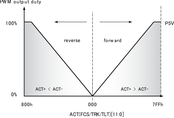 Figure 57. FCS/TRK/TLT Output Duty
9.1.12 Load Driver Part
The load driver outputs the voltage, with voltage feedback corresponding to the input DAC value. This channel has power voltage compensation and therefore is suited for slot-in type load control. This channel becomes active exclusively to other actuator channels. The load driver is shared with the TRK driver.
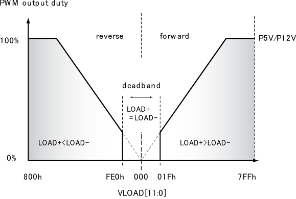 Figure 58. Load Output Duty
9.1.13 End Detect Function
This device has the function of end position detection for sled and collimator lens. This function eliminates the position switch at the PUH inner and collimator lens end position. Sled channel and step channel can be used independently by setting XXX_ENDDET_ENA = 1. When this function is enabled, internal logic detects the sled out zero-cross point, then the internal BEMF detect circuit measures the BEMF level of the stepping motor. There are four threshold levels. If the BEMF is lower than the selected threshold, the device causes the motor to stop and sets the XXX_ENDDET bit to 1. The ENDDET bit is then cleared at the BEMF voltage exceed threshold.
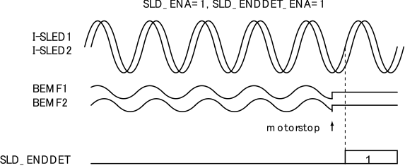 Figure 59. Timing of Sled End Detection
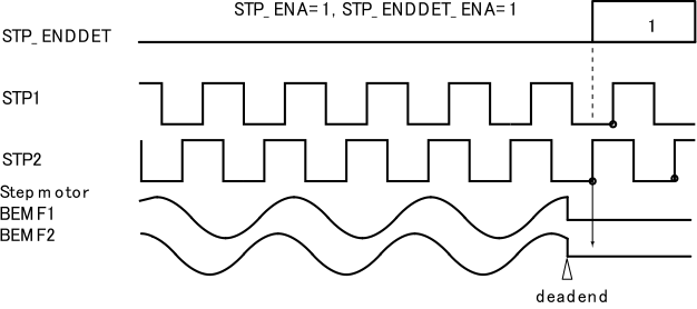 Figure 60. Timing of Step End Detection
9.1.14 Load Tray Lock Detect Function
The tray lock detect function detects inserted obstacles at the time of tray opening and closing, using the load motor BEMF. The user must adjust the TRAY_LOCKDET [2:0] for the optimal threshold level by the characteristics of the motor. By setting TRAY_LOCKDET, the user can select a threshold level from 100 to 400 mA, with a 50-mA step. Observe the lock detection by reading the TRAY_LOCKDETECT flag where LOAD_ENA = 1 is set.
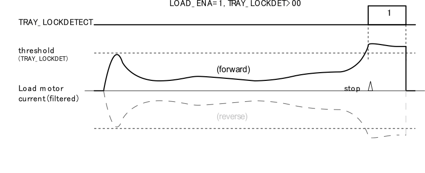 Figure 61. Load Tray Lock Detect
9.1.15 Load Tray Push Detect Function
The load tray can detect the event of push or pull using the TRAY_PUSHDETx flag. The push detect function monitors the motor BEMF voltage of LOAD_P and LOAD_N in the LOAD_ENA = 0. If the motor BEMF voltage exceeds the threshold level, the detection terminal flag is set where the voltage appeared. A detection threshold is determined by voltage (PUSHDETTH) and time (PUSHDET_TIME). Observe the push event by reading the TRAY_PUSHDETP or TRAY_PUSHDETN flags, where LOAD_ENA = 0 is set. Because TRAY_PUSHDETx is a latch flag, it is necessary to reset by RST_ERR_FLAG = 1.
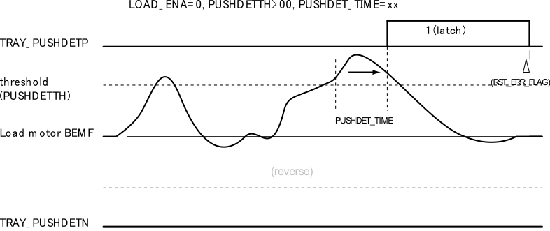 Figure 62. Load Tray Push Detect
9.1.16 Monitor Signal on GPOUT
The device can output a specific signal to the GPOUT pin. To output a signal, choose a signal from REG6F by enabling first, then enable GPOUT_ENA. When two or more signals are set for GPOUT, an output is a logical sum.
9.1.17 9-V LDO
The TPIC2060A has a built-in predriver for 9-V LDO. An arbitrary current can be supplied to the LDO by selecting the external NFET according to required current capacity. LIN9VG output (= NFET gate control) is controlled to the feedback voltage and LINFB is set as 1.215 V. The 220-nF capacitor for phase compensation is installed, and the division resistance for FB is chosen so that it may total less than 11 kΩ. Figure 63 shows an example of external components. The accuracy of the output voltage depends on the tolerance of the resistance. When not using the LDO, open both LIN9VG and LINFB with LIN9V_DISABLE = 1.
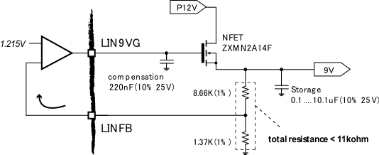 Figure 63. Example Circuit of 9-V LDO
9.2 Typical Application
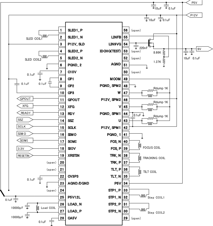 Figure 64. Example of Application Circuit
9.2.1 Design Requirements
To begin the design process, determine the following:
- Motor configuration. Can use all motor channels or part of them.
- Usage for 9V LDO predriver. Can be disabled.
- RDY pin can be connected to Host CPU. Then Host CPU can know the power supply status of TPIC2060A
9.2.2 Detailed Design Procedure
After power up on 5V and 12V supply, register can be changed following way and enabling motors.
- Set WRITE_ENABLE=1 on REG76 via SPI.
- Set XSLEEP=1 at REG70
- Enable motor channel by ENA_XXX bits on REG70
- Change the DAC settings for the motor on REG01-0B. Then output channels start driving load.
9.2.3 Application Curves
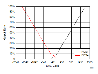 Figure 65. FCS Driver: DAC Code vs Output On Duty
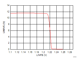 Figure 66. LDO Control: LINFB vs LIN9VG Output