SLOS704B January 2011 – August 2015 TPA6138A2
PRODUCTION DATA.
- 1 Features
- 2 Applications
- 3 Description
- 4 Revision History
- 5 Device Comparison Table
- 6 Pin Configuration and Functions
- 7 Specifications
- 8 Parameter Measurement Information
- 9 Detailed Description
- 10Application and Implementation
- 11Power Supply Recommendations
- 12Layout
- 13Device and Documentation Support
- 14Mechanical, Packaging, and Orderable Information
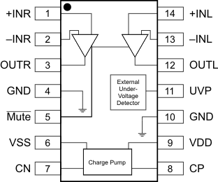
6 Pin Configuration and Functions
PW Package
14-Pin TSSOP
(Top View)

Pin Functions
| PIN | TYPE(1) | DESCRIPTION | ||
|---|---|---|---|---|
| NAME | NO. | |||
| CN | 7 | I/O | Charge-pump flying capacitor negative connection | |
| CP | 8 | I/O | Charge-pump flying capacitor positive connection | |
| GND | 4, 10 | P | Ground | |
| –INL | 13 | I | Left-channel OPAMP negative input | |
| +INL | 14 | I | Left-channel OPAMP positive input | |
| –INR | 2 | I | Right-channel OPAMP negative input | |
| +INR | 1 | I | Right-channel OPAMP positive input | |
| Mute | 5 | I | Mute, active-low | |
| OUTL | 12 | O | Left-channel OPAMP output | |
| OUTR | 3 | O | Right-channel OPAMP output | |
| UVP | 11 | I | Undervoltage protection; internal pull-up, unconnected if UVP function is unused. | |
| VDD | 9 | P | Positive supply | |
| VSS | 6 | P | Supply voltage | |
(1) I = input, O = output, P = power