ZHCSGF7B December   2008  – July 2017 TPA6132A2

PRODUCTION DATA.  

  1. 特性
  2. 应用范围
  3. 说明
  4. 修订历史记录
  5. Pin Configuration and Functions
  6. Specifications
    1. 6.1 Absolute Maximum Ratings
    2. 6.2 ESD Ratings
    3. 6.3 Recommended Operating Condtions
    4. 6.4 Thermal Information
    5. 6.5 Electrical Characteristics
    6. 6.6 Operating Characteristics
    7. 6.7 Typical Characteristics
  7. Detailed Description
    1. 7.1 Overview
    2. 7.2 Functional Block Diagram
    3. 7.3 Feature Description
      1. 7.3.1 Headphone Amplifiers
      2. 7.3.2 Eliminating Turn-on Pop and Power Supply Sequencing
      3. 7.3.3 RF and Power Supply Noise Immunity
      4. 7.3.4 Constant Maximum Output Power and Acoustic Shock Prevention
    4. 7.4 Device Functional Modes
      1. 7.4.1 Gain Control
  8. Application and Implementation
    1. 8.1 Application Information
    2. 8.2 Typical Applications
      1. 8.2.1 Configuration with Differential Input Signals
        1. 8.2.1.1 Design Requirements
        2. 8.2.1.2 Detailed Design Procedure
          1. 8.2.1.2.1 Input Coupling Capacitors
          2. 8.2.1.2.2 Charge Pump Flying Capacitor and HPVSS Capacitor
        3. 8.2.1.3 Application Curves
      2. 8.2.2 Configuration with Single-Ended Input Signals
        1. 8.2.2.1 Design Requirements
        2. 8.2.2.2 Detailed Design Procedure
        3. 8.2.2.3 Application Curves
  9. Power Supply Recommendations
    1. 9.1 Power Supply and HPVDD Decoupling Capacitors
  10. 10Layout
    1. 10.1 Layout Guidelines
    2. 10.2 Layout Example
    3. 10.3 GND Connections
  11. 11器件和文档支持
    1. 11.1 接收文档更新通知
    2. 11.2 社区资源
    3. 11.3 商标
    4. 11.4 静电放电警告
    5. 11.5 Glossary
  12. 12机械、封装和可订购信息

封装选项

请参考 PDF 数据表获取器件具体的封装图。

机械数据 (封装 | 引脚)
  • RTE|16
散热焊盘机械数据 (封装 | 引脚)
订购信息

Layout

Layout Guidelines

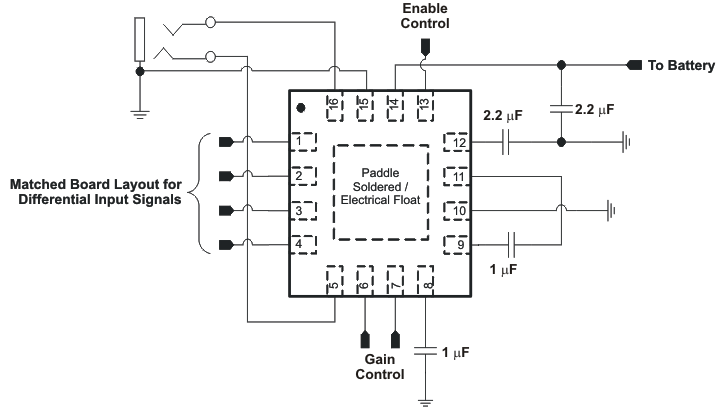
  • Solder the exposed metal pad on the TPA6132A2RTE QFN package to the landing pad on the PCB.
  • Connect the landing pad to ground or leave it electrically unconnected (floating). Do not connect the landing pad to VDD or to any other power supply voltage.
  • If the pad is grounded, it must be connected to the same ground as the PGND pin (10).
  • See the layout and mechanical drawings at the end of the data sheet for proper sizing.
  • Soldering the thermal pad is required for mechanical reliability and enhances thermal conductivity of the package.

WARNING

DO NOT connect the TPA6132A2RTE exposed metal pad to VDD or any other power supply voltage.

Layout Example

TPA6132A2 layout_los597.gif
Figure 30. Board Layout Concept

GND Connections

The SGND pin is an input reference and must be connected to the headphone ground connector pin. This ensures no turn-on pop and minimizes output offset voltage. Do not connect more than ±0.3 V to SGND.

PGND is a power ground. Connect supply decoupling capacitors for VDD, HPVDD, and HPVSS to PGND.