SLOS488F November   2006  – March 2015 TPA6130A2

PRODUCTION DATA.  

  1. Features
  2. Applications
  3. Description
  4. Simplified Schematic
  5. Revision History
  6. Pin Configuration and Functions
  7. Specifications
    1. 7.1 Absolute Maximum Ratings
    2. 7.2 Handling Ratings
    3. 7.3 Recommended Operating Conditions
    4. 7.4 Thermal Information
    5. 7.5 Electrical Characteristics
    6. 7.6 Operating Characteristics
    7. 7.7 Timing Requirements
    8. 7.8 Typical Characteristics
  8. Detailed Description
    1. 8.1 Overview
    2. 8.2 Functional Block Diagram
    3. 8.3 Feature Description
      1. 8.3.1 Headphone Amplifiers
    4. 8.4 Device Functional Modes
      1. 8.4.1 Hardware Shutdown
      2. 8.4.2 Software Shutdown
      3. 8.4.3 Charge Pump Enabled, HP Amplifiers Disabled
      4. 8.4.4 Hi-Z State
      5. 8.4.5 Stereo Headphone Drive
      6. 8.4.6 Dual Mono Headphone Drive
      7. 8.4.7 Bridge-Tied Load Receiver Drive
      8. 8.4.8 Default Mode
      9. 8.4.9 Volume Control
    5. 8.5 Programming
      1. 8.5.1 General I2C Operation
      2. 8.5.2 Single-and Multiple-Byte Transfers
      3. 8.5.3 Single-Byte Write
      4. 8.5.4 Multiple-Byte Write and Incremental Multiple-Byte Write
      5. 8.5.5 Single-Byte Read
      6. 8.5.6 Multiple-Byte Read
    6. 8.6 Register Maps
      1. 8.6.1 Control Register (Address: 1)
      2. 8.6.2 Volume and Mute Register (Address: 2)
      3. 8.6.3 Output Impedance Register (Address: 3)
      4. 8.6.4 I2C address and Version Register (Address: 4)
      5. 8.6.5 Reserved for test registers (Addresses: 5-8)
  9. Applications and Implementation
    1. 9.1 Application Information
    2. 9.2 Typical Application
      1. 9.2.1 Design Requirements
      2. 9.2.2 Detailed Design Procedure
        1. 9.2.2.1 Input-Blocking Capacitors
        2. 9.2.2.2 Charge Pump Flying Capacitor and CPVSS Capacitor
        3. 9.2.2.3 Decoupling Capacitors
        4. 9.2.2.4 I2C Control Interface Details
          1. 9.2.2.4.1 Addressing the TPA6130A2
        5. 9.2.2.5 Headphone Amplifiers
      3. 9.2.3 Application Performance Curves
  10. 10Power Supply Recommendations
  11. 11Layout
    1. 11.1 Layout Guidelines
    2. 11.2 Layout Example
  12. 12Device and Documentation Support
    1. 12.1 Trademarks
    2. 12.2 Electrostatic Discharge Caution
    3. 12.3 Glossary
  13. 13Mechanical, Packaging, and Orderable Information

封装选项

机械数据 (封装 | 引脚)
散热焊盘机械数据 (封装 | 引脚)
订购信息

11 Layout

11.1 Layout Guidelines

Exposed Pad On TPA6130A2RTJ Package Option:

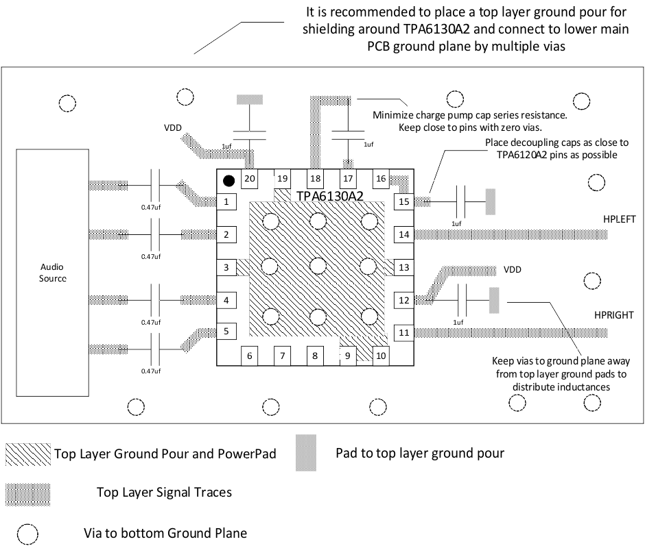
  • Solder the exposed metal pad on the TPA6130A2RTJ QFN package to the a pad on the PCB. The pad on the PCB may be grounded or may be allowed to float (not be connected to ground or power).
  • If the pad is grounded, it must be connected to the same ground as the GND pins (3, 9, 10, 13, and 19).
  • Soldering the thermal pad improves mechanical reliability, improves grounding of the device, and enhances thermal conductivity of the package.

GND Connections:

  • The GND pin for charge pump should be decoupled to the charge pump VDD pin, and the GND pin adjacent to the Analog VDD pin should be separately decoupled to each other.

11.2 Layout Example
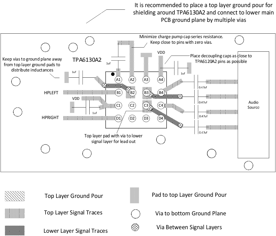
TPA6130A2 Layout_Example_YZH_slos488.gifFigure 48. YZH (DSBGA) Package
TPA6130A2 Layout_Example_RTJ_slos488.gifFigure 49. RTJ (WQFN) Package