ZHCSA13P November 2008 – February 2021 TMS320F28020 , TMS320F280200 , TMS320F28021 , TMS320F28022 , TMS320F28023 , TMS320F28023-Q1 , TMS320F28026 , TMS320F28026-Q1 , TMS320F28026F , TMS320F28027 , TMS320F28027-Q1 , TMS320F28027F , TMS320F28027F-Q1
PRODUCTION DATA
- 1 特性
- 2 应用
- 3 说明
- 4 功能方框图
- 5 修订历史记录
- 6 Device Comparison
- 7 Terminal Configuration and Functions
- 8 规格
-
9 详细说明
- 9.1
Overview
- 9.1.1 CPU
- 9.1.2 Memory Bus (Harvard Bus Architecture)
- 9.1.3 外设总线
- 9.1.4 Real-Time JTAG and Analysis
- 9.1.5 Flash
- 9.1.6 M0,M1 SARAM
- 9.1.7 L0 SARAM
- 9.1.8 Boot ROM
- 9.1.9 Security
- 9.1.10 外设中断扩展 (PIE) 块
- 9.1.11 外部中断 (XINT1-XINT3)
- 9.1.12 内部零引脚振荡器、振荡器和 PLL
- 9.1.13 看门狗
- 9.1.14 Peripheral Clocking
- 9.1.15 Low-power Modes
- 9.1.16 外设帧 0,1,2 (PFn)
- 9.1.17 通用输入/输出 (GPIO) 复用器
- 9.1.18 32 位 CPU 定时器 (0,1,2)
- 9.1.19 Control Peripherals
- 9.1.20 串行端口外设
- 9.2 Memory Maps
- 9.3 Register Maps
- 9.4 Device Emulation Registers
- 9.5 VREG/BOR/POR
- 9.6 系统控制
- 9.7 Low-power Modes Block
- 9.8 Interrupts
- 9.9
外设
- 9.9.1 Analog Block
- 9.9.2 详细说明
- 9.9.3 Serial Peripheral Interface (SPI) Module
- 9.9.4 Serial Communications Interface (SCI) Module
- 9.9.5 Inter-Integrated Circuit (I2C)
- 9.9.6 Enhanced PWM Modules (ePWM1/2/3/4)
- 9.9.7 High-Resolution PWM (HRPWM)
- 9.9.8 Enhanced Capture Module (eCAP1)
- 9.9.9 JTAG 端口
- 9.9.10 General-Purpose Input/Output (GPIO) MUX
- 9.1
Overview
- 10应用、实施和布局
- 11器件和文档支持
- 12机械、封装和可订购信息
9.2 Memory Maps
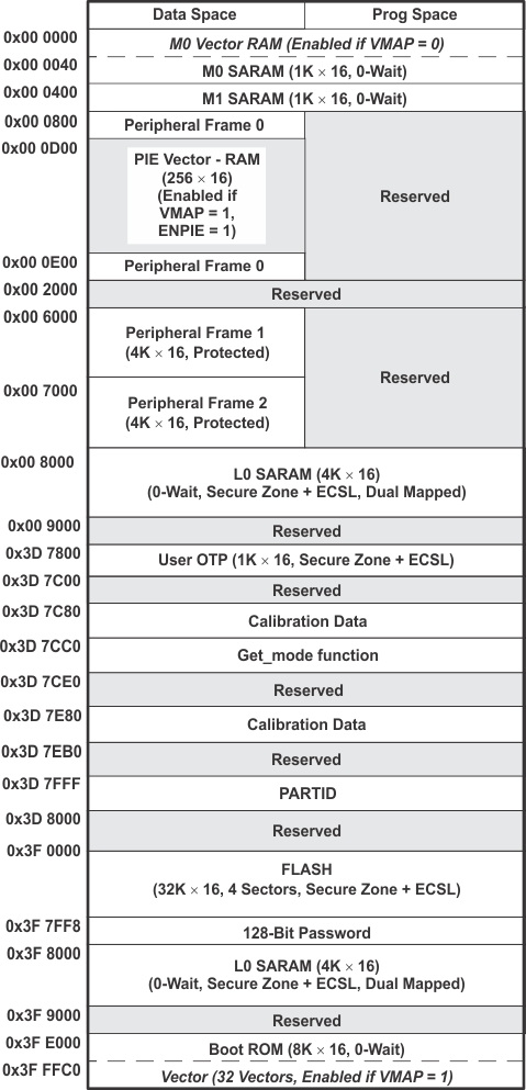
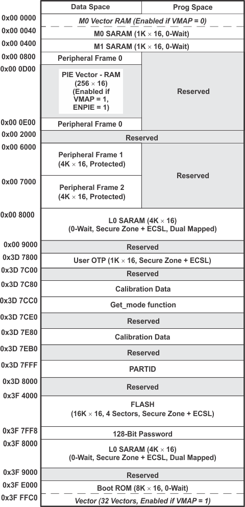
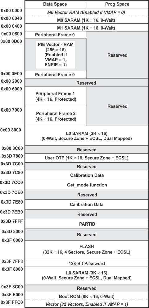
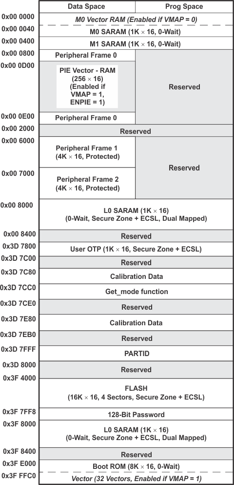
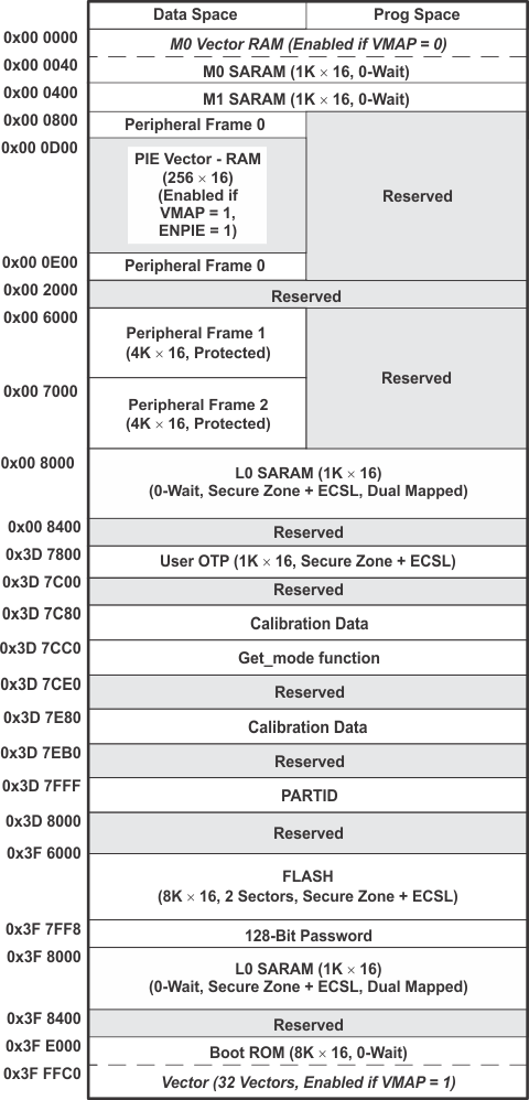
In Figure 9-1, Figure 9-2, Figure 9-3, Figure 9-4, and Figure 9-5, the following apply:
- Memory blocks are not to scale.
- Peripheral Frame 0, Peripheral Frame 1 and Peripheral Frame 2 memory maps are restricted to data memory only. A user program cannot access these memory maps in program space.
- Protected means the order of Write-followed-by-Read operations is preserved rather than the pipeline order.
- Certain memory ranges are EALLOW protected against spurious writes after configuration.
- Locations 0x3D7C80 to 0x3D7CC0 contain the internal oscillator and ADC calibration routines. These locations are not programmable by the user.
| ADDRESS RANGE | PROGRAM AND DATA SPACE |
|---|---|
| 0x3F 0000 to 0x3F 1FFF | Sector D (8K × 16) |
| 0x3F 2000 to 0x3F 3FFF | Sector C (8K × 16) |
| 0x3F 4000 to 0x3F 5FFF | Sector B (8K × 16) |
| 0x3F 6000 to 0x3F 7F7F | Sector A (8K × 16) |
| 0x3F 7F80 to 0x3F 7FF5 | Program to 0x0000 when using the Code Security Module |
| 0x3F 7FF6 to 0x3F 7FF7 | Boot-to-Flash Entry Point (program branch instruction here) |
| 0x3F 7FF8 to 0x3F 7FFF | Security
Password (128-Bit) (Do not program to all zeros) |
| ADDRESS RANGE | PROGRAM AND DATA SPACE |
|---|---|
| 0x3F 4000 to 0x3F 4FFF | Sector D (4K × 16) |
| 0x3F 5000 to 0x3F 5FFF | Sector C (4K × 16) |
| 0x3F 6000 to 0x3F 6FFF | Sector B (4K × 16) |
| 0x3F 7000 to 0x3F 7F7F | Sector A (4K × 16) |
| 0x3F 7F80 to 0x3F 7FF5 | Program to 0x0000 when using the Code Security Module |
| 0x3F 7FF6 to 0x3F 7FF7 | Boot-to-Flash Entry Point (program branch instruction here) |
| 0x3F 7FF8 to 0x3F 7FFF | Security Password (128-Bit) (Do not program to all zeros) |
| ADDRESS RANGE | PROGRAM AND DATA SPACE |
|---|---|
| 0x3F 6000 to 0x3F 6FFF | Sector B (4K × 16) |
| 0x3F 7000 to 0x3F 7F7F | Sector A (4K × 16) |
| 0x3F 7F80 to 0x3F 7FF5 | Program to 0x0000 when using the Code Security Module |
| 0x3F 7FF6 to 0x3F 7FF7 | Boot-to-Flash Entry Point (program branch instruction here) |
| 0x3F 7FF8 to 0x3F 7FFF | Security Password (128-Bit) (Do not program to all zeros) |
- When the code-security passwords are programmed, all addresses from 0x3F 7F80 to 0x3F 7FF5 cannot be used as program code or data. These locations must be programmed to 0x0000.
- If the code security feature is not used, addresses 0x3F 7F80 to 0x3F 7FEF may be used for code or data. Addresses 0x3F 7FF0 to 0x3F 7FF5 are reserved for data and should not contain program code.
Table 9-6 shows how to handle these memory locations.
| ADDRESS | FLASH | |
|---|---|---|
| CODE SECURITY ENABLED | CODE SECURITY DISABLED | |
| 0x3F 7F80 to 0x3F 7FEF | Fill with 0x0000 | Application code and data |
| 0x3F 7FF0 to 0x3F 7FF5 | Reserved for data only | |
Peripheral Frame 1 and Peripheral Frame 2 are grouped together to enable these blocks to be write/read peripheral block protected. The protected mode makes sure that all accesses to these blocks happen as written. Because of the pipeline, a write immediately followed by a read to different memory locations, will appear in reverse order on the memory bus of the CPU. This can cause problems in certain peripheral applications where the user expected the write to occur first (as written). The CPU supports a block protection mode where a region of memory can be protected so that operations occur as written (the penalty is extra cycles are added to align the operations). This mode is programmable and by default, it protects the selected zones.
The wait states for the various spaces in the memory map area are listed in Table 9-7.
| AREA | WAIT STATES (CPU) | COMMENTS |
|---|---|---|
| M0 and M1 SARAMs | 0-wait | Fixed |
| Peripheral Frame 0 | 0-wait | |
| Peripheral Frame 1 | 0-wait (writes) | Cycles can be extended by peripheral generated ready. |
| 2-wait (reads) | Back-to-back write operations to Peripheral Frame 1 registers will incur a 1-cycle stall (1-cycle delay). | |
| Peripheral Frame 2 | 0-wait (writes) | Fixed. Cycles cannot be extended by the peripheral. |
| 2-wait (reads) | ||
| L0 SARAM | 0-wait data and program | Assumes no CPU conflicts |
| OTP | Programmable | Programmed through the Flash registers. |
| 1-wait minimum | 1-wait is minimum number of wait states allowed. | |
| FLASH | Programmable | Programmed through the Flash registers. |
| 0-wait Paged min | ||
| 1-wait Random min Random ≥ Paged | ||
| FLASH Password | 16-wait fixed | Wait states of password locations are fixed. |
| Boot-ROM | 0-wait |