ZHCSGV6F June 2009 – January 2017 TMS320C6742
PRODUCTION DATA.
- 1器件概述
- 2Revision History
-
3Device Comparison
- 3.1 Device Characteristics
- 3.2 Device Compatibility
- 3.3 DSP Subsystem
- 3.4 Memory Map Summary
- 3.5 Pin Assignments
- 3.6 Pin Multiplexing Control
- 3.7
Terminal Functions
- 3.7.1 Device Reset, NMI and JTAG
- 3.7.2 High-Frequency Oscillator and PLL
- 3.7.3 Real-Time Clock and 32-kHz Oscillator
- 3.7.4 DEEPSLEEP Power Control
- 3.7.5 External Memory Interface A (EMIFA)
- 3.7.6 DDR2/mDDR Controller
- 3.7.7 Serial Peripheral Interface Modules (SPI)
- 3.7.8 Enhanced Capture/Auxiliary PWM Modules (eCAP0)
- 3.7.9 Enhanced Pulse Width Modulators (eHRPWM)
- 3.7.10 Boot
- 3.7.11 Universal Asynchronous Receiver/Transmitters (UART0)
- 3.7.12 Inter-Integrated Circuit Modules(I2C0)
- 3.7.13 Timers
- 3.7.14 Multichannel Audio Serial Ports (McASP)
- 3.7.15 Multichannel Buffered Serial Ports (McBSP)
- 3.7.16 Universal Host-Port Interface (UHPI)
- 3.7.17 General Purpose Input Output
- 3.7.18 Reserved and No Connect
- 3.7.19 Supply and Ground
- 3.8 Unused Pin Configurations
- 4Device Configuration
-
5Specifications
- 5.1 Absolute Maximum Ratings Over Operating Junction Temperature Range (Unless Otherwise Noted)
- 5.2 Handling Ratings
- 5.3 Recommended Operating Conditions
- 5.4 Notes on Recommended Power-On Hours (POH)
- 5.5 Electrical Characteristics Over Recommended Ranges of Supply Voltage and Operating Junction Temperature (Unless Otherwise Noted)
-
6Peripheral Information and Electrical Specifications
- 6.1 Parameter Information
- 6.2 Recommended Clock and Control Signal Transition Behavior
- 6.3 Power Supplies
- 6.4 Reset
- 6.5 Crystal Oscillator or External Clock Input
- 6.6 Clock PLLs
- 6.7 Interrupts
- 6.8 Power and Sleep Controller (PSC)
- 6.9 Enhanced Direct Memory Access Controller (EDMA3)
- 6.10 External Memory Interface A (EMIFA)
- 6.11
DDR2/mDDR Memory Controller
- 6.11.1 DDR2/mDDR Memory Controller Electrical Data/Timing
- 6.11.2 DDR2/mDDR Memory Controller Register Description(s)
- 6.11.3
DDR2/mDDR Interface
- 6.11.3.1 DDR2/mDDR Interface Schematic
- 6.11.3.2 Compatible JEDEC DDR2/mDDR Devices
- 6.11.3.3 PCB Stackup
- 6.11.3.4 Placement
- 6.11.3.5 DDR2/mDDR Keep Out Region
- 6.11.3.6 Bulk Bypass Capacitors
- 6.11.3.7 High-Speed Bypass Capacitors
- 6.11.3.8 Net Classes
- 6.11.3.9 DDR2/mDDR Signal Termination
- 6.11.3.10 VREF Routing
- 6.11.3.11 DDR2/mDDR CK and ADDR_CTRL Routing
- 6.11.3.12 DDR2/mDDR Boundary Scan Limitations
- 6.12 Memory Protection Units
- 6.13 Multichannel Audio Serial Port (McASP)
- 6.14
Multichannel Buffered Serial Port (McBSP)
- 6.14.1 McBSP Peripheral Register Description(s)
- 6.14.2
McBSP Electrical Data/Timing
- 6.14.2.1
Multichannel Buffered Serial Port (McBSP) Timing
- Table 6-47 Timing Requirements for McBSP1 [1.2V, 1.1V] (see )
- Table 6-48 Timing Requirements for McBSP1 [1.0V] (see )
- Table 6-49 Switching Characteristics for McBSP1 [1.2V, 1.1V] (see )
- Table 6-50 Switching Characteristics for McBSP1 [1.0V] (see )
- Table 6-51 Timing Requirements for McBSP1 FSR When GSYNC = 1 (see )
- 6.14.2.1
Multichannel Buffered Serial Port (McBSP) Timing
- 6.15 Serial Peripheral Interface Ports (SPI1)
- 6.16 Inter-Integrated Circuit Serial Ports (I2C)
- 6.17 Universal Asynchronous Receiver/Transmitter (UART)
- 6.18 Host-Port Interface (UHPI)
- 6.19 Enhanced Capture (eCAP) Peripheral
- 6.20 Enhanced High-Resolution Pulse-Width Modulator (eHRPWM)
- 6.21 Timers
- 6.22 Real Time Clock (RTC)
- 6.23 General-Purpose Input/Output (GPIO)
- 6.24 Emulation Logic
- 7Device and Documentation Support
- 8Mechanical Packaging and Orderable Information
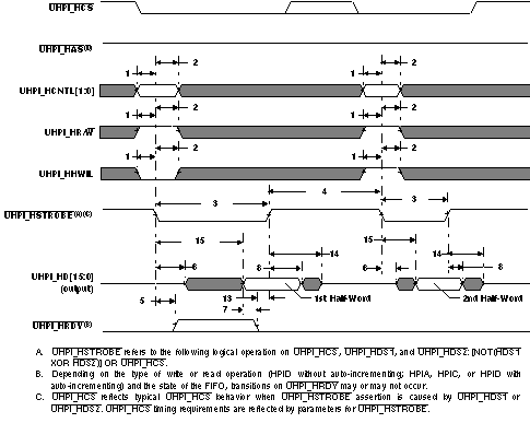
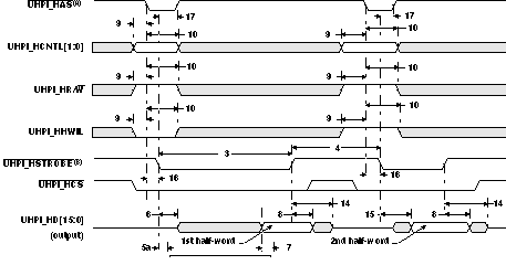
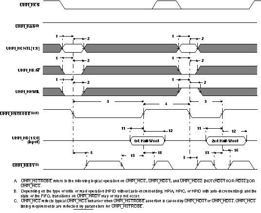
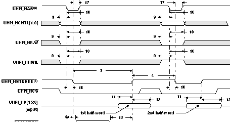
Table 6-70 Switching Characteristics Over Recommended Operating Conditions for Host-Port Interface [1.0V](1)(2)(3)
| NO. | PARAMETER | 1.0V | UNIT | |||
|---|---|---|---|---|---|---|
| MIN | MAX | |||||
| 5 | td(HSTBL-HRDYV) | Delay time, HSTROBE low to HRDY valid | For HPI Write, HRDY can go high (not ready) for these HPI Write conditions; otherwise, HRDY stays low (ready):
Case 1: Back-to-back HPIA writes (can be either first or second half-word) Case 2: HPIA write following a PREFETCH command (can be either first or second half-word) Case 3: HPID write when FIFO is full or flushing (can be either first or second half-word) Case 4: HPIA write and Write FIFO not empty For HPI Read, HRDY can go high (not ready) for these HPI Read conditions: Case 1: HPID read (with auto-increment) and data not in Read FIFO (can only happen to first half-word of HPID access) Case 2: First half-word access of HPID Read without auto-increment For HPI Read, HRDY stays low (ready) for these HPI Read conditions: Case 1: HPID read with auto-increment and data is already in Read FIFO (applies to either half-word of HPID access) Case 2: HPID read without auto-increment and data is already in Read FIFO (always applies to second half-word of HPID access) Case 3: HPIC or HPIA read (applies to either half-word access) |
22 | ns | |
| 5a | td(HASL-HRDYV) | Delay time, HAS low to HRDY valid | 22 | ns | ||
| 6 | ten(HSTBL-HDLZ) | Enable time, HD driven from HSTROBE low | 1.5 | ns | ||
| 7 | td(HRDYL-HDV) | Delay time, HRDY low to HD valid | 0 | ns | ||
| 8 | toh(HSTBH-HDV) | Output hold time, HD valid after HSTROBE high | 1.5 | ns | ||
| 14 | tdis(HSTBH-HDHZ) | Disable time, HD high-impedance from HSTROBE high | 22 | ns | ||
| 15 | td(HSTBL-HDV) | Delay time, HSTROBE low to HD valid | For HPI Read. Applies to conditions where data is already residing in HPID/FIFO:
Case 1: HPIC or HPIA read Case 2: First half-word of HPID read with auto-increment and data is already in Read FIFO Case 3: Second half-word of HPID read with or without auto-increment |
22 | ns | |
| 18 | td(HSTBH-HRDYV) | Delay time, HSTROBE high to HRDY valid | For HPI Write, HRDY can go high (not ready) for these HPI Write conditions; otherwise, HRDY stays low (ready):
Case 1: HPID write when Write FIFO is full (can happen to either half-word) Case 2: HPIA write (can happen to either half-word) Case 3: HPID write without auto-increment (only happens to second half-word) |
22 | ns | |
(1) M=SYSCLK2 period in ns.
(2) HSTROBE refers to the following logical operation on HCS, HDS1, and HDS2: [NOT(HDS1 XOR HDS2)] OR HCS.
(3) By design, whenever HCS is driven inactive (high), HPI will drive HRDY active (low).
 Figure 6-41 UHPI Read Timing (HAS Not Used, Tied High)

A. For correct operation, strobe the UHPI_HAS signal only once per UHPI_HSTROBE active cycle.
B. UHPI_HSTROBE refers to the following logical operation on UHPI_HCS, UHPI_HDS1, and UHPI_HDS2: [NOT(UHPI_HDS1 XOR UHPI_HDS2)] OR UHPI_HCS.
Figure 6-42 UHPI Read Timing (HAS Used)
 Figure 6-43 UHPI Write Timing (HAS Not Used, Tied High)

A. For correct operation, strobe the UHPI_HAS signal only once per UHPI_HSTROBE active cycle.
B. UHPI_HSTROBE refers to the following logical operation on UHPI_HCS, UHPI_HDS1, and UHPI_HDS2: [NOT(UHPI_HDS1 XOR UHPI_HDS2)] OR UHPI_HCS.
Figure 6-44 UHPI Write Timing (HAS Used)