ZHCSGV6F June 2009 – January 2017 TMS320C6742
PRODUCTION DATA.
- 1器件概述
- 2Revision History
-
3Device Comparison
- 3.1 Device Characteristics
- 3.2 Device Compatibility
- 3.3 DSP Subsystem
- 3.4 Memory Map Summary
- 3.5 Pin Assignments
- 3.6 Pin Multiplexing Control
- 3.7
Terminal Functions
- 3.7.1 Device Reset, NMI and JTAG
- 3.7.2 High-Frequency Oscillator and PLL
- 3.7.3 Real-Time Clock and 32-kHz Oscillator
- 3.7.4 DEEPSLEEP Power Control
- 3.7.5 External Memory Interface A (EMIFA)
- 3.7.6 DDR2/mDDR Controller
- 3.7.7 Serial Peripheral Interface Modules (SPI)
- 3.7.8 Enhanced Capture/Auxiliary PWM Modules (eCAP0)
- 3.7.9 Enhanced Pulse Width Modulators (eHRPWM)
- 3.7.10 Boot
- 3.7.11 Universal Asynchronous Receiver/Transmitters (UART0)
- 3.7.12 Inter-Integrated Circuit Modules(I2C0)
- 3.7.13 Timers
- 3.7.14 Multichannel Audio Serial Ports (McASP)
- 3.7.15 Multichannel Buffered Serial Ports (McBSP)
- 3.7.16 Universal Host-Port Interface (UHPI)
- 3.7.17 General Purpose Input Output
- 3.7.18 Reserved and No Connect
- 3.7.19 Supply and Ground
- 3.8 Unused Pin Configurations
- 4Device Configuration
-
5Specifications
- 5.1 Absolute Maximum Ratings Over Operating Junction Temperature Range (Unless Otherwise Noted)
- 5.2 Handling Ratings
- 5.3 Recommended Operating Conditions
- 5.4 Notes on Recommended Power-On Hours (POH)
- 5.5 Electrical Characteristics Over Recommended Ranges of Supply Voltage and Operating Junction Temperature (Unless Otherwise Noted)
-
6Peripheral Information and Electrical Specifications
- 6.1 Parameter Information
- 6.2 Recommended Clock and Control Signal Transition Behavior
- 6.3 Power Supplies
- 6.4 Reset
- 6.5 Crystal Oscillator or External Clock Input
- 6.6 Clock PLLs
- 6.7 Interrupts
- 6.8 Power and Sleep Controller (PSC)
- 6.9 Enhanced Direct Memory Access Controller (EDMA3)
- 6.10 External Memory Interface A (EMIFA)
- 6.11
DDR2/mDDR Memory Controller
- 6.11.1 DDR2/mDDR Memory Controller Electrical Data/Timing
- 6.11.2 DDR2/mDDR Memory Controller Register Description(s)
- 6.11.3
DDR2/mDDR Interface
- 6.11.3.1 DDR2/mDDR Interface Schematic
- 6.11.3.2 Compatible JEDEC DDR2/mDDR Devices
- 6.11.3.3 PCB Stackup
- 6.11.3.4 Placement
- 6.11.3.5 DDR2/mDDR Keep Out Region
- 6.11.3.6 Bulk Bypass Capacitors
- 6.11.3.7 High-Speed Bypass Capacitors
- 6.11.3.8 Net Classes
- 6.11.3.9 DDR2/mDDR Signal Termination
- 6.11.3.10 VREF Routing
- 6.11.3.11 DDR2/mDDR CK and ADDR_CTRL Routing
- 6.11.3.12 DDR2/mDDR Boundary Scan Limitations
- 6.12 Memory Protection Units
- 6.13 Multichannel Audio Serial Port (McASP)
- 6.14
Multichannel Buffered Serial Port (McBSP)
- 6.14.1 McBSP Peripheral Register Description(s)
- 6.14.2
McBSP Electrical Data/Timing
- 6.14.2.1
Multichannel Buffered Serial Port (McBSP) Timing
- Table 6-47 Timing Requirements for McBSP1 [1.2V, 1.1V] (see )
- Table 6-48 Timing Requirements for McBSP1 [1.0V] (see )
- Table 6-49 Switching Characteristics for McBSP1 [1.2V, 1.1V] (see )
- Table 6-50 Switching Characteristics for McBSP1 [1.0V] (see )
- Table 6-51 Timing Requirements for McBSP1 FSR When GSYNC = 1 (see )
- 6.14.2.1
Multichannel Buffered Serial Port (McBSP) Timing
- 6.15 Serial Peripheral Interface Ports (SPI1)
- 6.16 Inter-Integrated Circuit Serial Ports (I2C)
- 6.17 Universal Asynchronous Receiver/Transmitter (UART)
- 6.18 Host-Port Interface (UHPI)
- 6.19 Enhanced Capture (eCAP) Peripheral
- 6.20 Enhanced High-Resolution Pulse-Width Modulator (eHRPWM)
- 6.21 Timers
- 6.22 Real Time Clock (RTC)
- 6.23 General-Purpose Input/Output (GPIO)
- 6.24 Emulation Logic
- 7Device and Documentation Support
- 8Mechanical Packaging and Orderable Information
6.11.3.11 DDR2/mDDR CK and ADDR_CTRL Routing
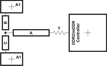
Figure 6-23 shows the topology of the routing for the CK and ADDR_CTRL net classes. The route is a balanced T as it is intended that the length of segments B and C be equal. In addition, the length of A should be maximized.
 Figure 6-23 CK and ADDR_CTRL Routing and Topology
Table 6-34 CK and ADDR_CTRL Routing Specification
| NO. | PARAMETER | MIN | TYP | MAX | UNIT |
|---|---|---|---|---|---|
| 1 | Center to Center CK-CKN Spacing(3) | 2w(4) | |||
| 2 | CK A to B/A to C Skew Length Mismatch(1) | 25 | Mils | ||
| 3 | CK B to C Skew Length Mismatch | 25 | Mils | ||
| 4 | Center to center CK to other DDR2/mDDR trace spacing(3) | 4w(4) | |||
| 5 | CK/ADDR_CTRL nominal trace length(2) | CACLM-50 | CACLM | CACLM+50 | Mils |
| 6 | ADDR_CTRL to CK Skew Length Mismatch | 100 | Mils | ||
| 7 | ADDR_CTRL to ADDR_CTRL Skew Length Mismatch | 100 | Mils | ||
| 8 | Center to center ADDR_CTRL to other DDR2/mDDR trace spacing(3) | 4w(4) | |||
| 9 | Center to center ADDR_CTRL to other ADDR_CTRL trace spacing(3) | 3w (4) | |||
| 10 | ADDR_CTRL A to B/A to C Skew Length Mismatch(1) | 100 | Mils | ||
| 11 | ADDR_CTRL B to C Skew Length Mismatch | 100 | Mils |
(1) Series terminator, if used, should be located closest to device.
(2) CACLM is the longest Manhattan distance of the CK and ADDR_CTRL net classes.
(3) Center to center spacing is allowed to fall to minimum (w) for up to 500 mils of routed length to accommodate BGA escape and routing congestion.
(4) w = PCB trace width as defined in Table 6-27.
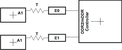
Figure 6-24 shows the topology and routing for the DQS and D net class; the routes are point to point. Skew matching across bytes is not needed nor recommended.
 Figure 6-24 DQS and D Routing and Topology
Table 6-35 DQS and D Routing Specification
| NO. | PARAMETER | MIN | TYP | MAX | UNIT |
|---|---|---|---|---|---|
| 1 | Center to center DQS to other DDR2/mDDR trace spacing(4) | 4w(6) | |||
| 2 | DQS/D nominal trace length(1)(3) | DQLM-50 | DQLM | DQLM+50 | Mils |
| 3 | D to DQS Skew Length Mismatch(3) | 100 | Mils | ||
| 4 | D to D Skew Length Mismatch(3) | 100 | Mils | ||
| 5 | Center to center D to other DDR2/mDDR trace spacing(4)(5) | 4w(6) | |||
| 6 | Center to Center D to other D trace spacing(4)(2) | 3w(6) |
(1) Series terminator, if used, should be located closest to DDR.
(2) DQLM is the longest Manhattan distance of each of the DQS and D net class.
(3) There is no need and it is not recommended to skew match across data bytes, i.e., from DQS0 and data byte 0 to DQS1 and data byte 1.
(4) Center to center spacing is allowed to fall to minimum (w) for up to 500 mils of routed length to accommodate BGA escape and routing congestion.
(5) D's from other DQS domains are considered other DDR2/mDDR trace.
(6) w = PCB trace width as defined in Table 6-27.
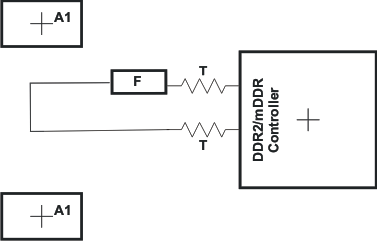
Figure 6-25 shows the routing for the DQGATE net class. Table 6-36 contains the routing specification.
 Figure 6-25 DQGATE Routing
Table 6-36 DQGATE Routing Specification
| NO. | PARAMETER | MIN | TYP | MAX | UNIT |
|---|---|---|---|---|---|
| 1 | DQGATE Length F | CKB0B(1) | |||
| 2 | Center to center DQGATE to any other trace spacing | 4w(3) | |||
| 3 | DQS/D nominal trace length | DQLM-50 | DQLM | DQLM+50 | Mils |
| 4 | DQGATE Skew(2) | 100 | Mils |
(1) CKB0B1 is the sum of the length of the CK net plus the average length of the DQS0 and DQS1 nets.
(2) Skew from CKB0B1
(3) w = PCB trace width as defined in Table 6-27.