ZHCSJ34F December 2015 – May 2019 TDA2HF , TDA2HG , TDA2HV , TDA2LF , TDA2SA , TDA2SG , TDA2SX
PRODUCTION DATA.
- 1 器件概述
- 2 修订历史记录
- 3 Device Comparison
-
4 Terminal Configuration and Functions
- 4.1 Terminal Assignment
- 4.2 Ball Characteristics
- 4.3 Multiplexing Characteristics
- 4.4
Signal Descriptions
- 4.4.1 Video Input Port (VIP)
- 4.4.2 Display Subsystem – Video Output Ports
- 4.4.3 Display Subsystem – High-Definition Multimedia Interface (HDMI)
- 4.4.4 External Memory Interface (EMIF)
- 4.4.5 General-Purpose Memory Controller (GPMC)
- 4.4.6 Timers
- 4.4.7 Inter-Integrated Circuit Interface (I2C)
- 4.4.8 Universal Asynchronous Receiver Transmitter (UART)
- 4.4.9 Multichannel Serial Peripheral Interface (McSPI)
- 4.4.10 Quad Serial Peripheral Interface (QSPI)
- 4.4.11 Multichannel Audio Serial Port (McASP)
- 4.4.12 Universal Serial Bus (USB)
- 4.4.13 SATA
- 4.4.14 Peripheral Component Interconnect Express (PCIe)
- 4.4.15 Controller Area Network Interface (DCAN)
- 4.4.16 Ethernet Interface (GMAC_SW)
- 4.4.17 eMMC/SD/SDIO
- 4.4.18 General-Purpose Interface (GPIO)
- 4.4.19 Pulse Width Modulation (PWM) Interface
- 4.4.20 System and Miscellaneous
- 4.4.21 Test Interfaces
-
5 Specifications
- 5.1 Absolute Maximum Ratings
- 5.2 ESD Ratings
- 5.3 Power on Hour (POH) Limits
- 5.4 Recommended Operating Conditions
- 5.5 Operating Performance Points
- 5.6 Power Consumption Summary
- 5.7
Electrical Characteristics
- 5.7.1 LVCMOS DDR DC Electrical Characteristics
- 5.7.2 HDMIPHY DC Electrical Characteristics
- 5.7.3 Dual Voltage LVCMOS I2C DC Electrical Characteristics
- 5.7.4 IQ1833 Buffers DC Electrical Characteristics
- 5.7.5 IHHV1833 Buffers DC Electrical Characteristics
- 5.7.6 LVCMOS OSC Buffers DC Electrical Characteristics
- 5.7.7 BC1833IHHV Buffers DC Electrical Characteristics
- 5.7.8 USBPHY DC Electrical Characteristics
- 5.7.9 Dual Voltage SDIO1833 DC Electrical Characteristics
- 5.7.10 Dual Voltage LVCMOS DC Electrical Characteristics
- 5.7.11 SATAPHY DC Electrical Characteristics
- 5.7.12 PCIEPHY DC Electrical Characteristics
- 5.8 Thermal Resistance Characteristics
- 5.9 Power Supply Sequences
- 6 Clock Specifications
-
7 Timing Requirements and Switching Characteristics
- 7.1 Timing Test Conditions
- 7.2 Interface Clock Specifications
- 7.3 Timing Parameters and Information
- 7.4 Recommended Clock and Control Signal Transition Behavior
- 7.5 Virtual and Manual I/O Timing Modes
- 7.6 Video Input Ports (VIP)
- 7.7 Display Subsystem – Video Output Ports
- 7.8 Display Subsystem – High-Definition Multimedia Interface (HDMI)
- 7.9 External Memory Interface (EMIF)
- 7.10 General-Purpose Memory Controller (GPMC)
- 7.11 Timers
- 7.12 Inter-Integrated Circuit Interface (I2C)
- 7.13 Universal Asynchronous Receiver Transmitter (UART)
- 7.14 Multichannel Serial Peripheral Interface (McSPI)
- 7.15 Quad Serial Peripheral Interface (QSPI)
- 7.16
Multichannel Audio Serial Port (McASP)
- Table 7-45 Timing Requirements for McASP1
- Table 7-46 Timing Requirements for McASP2
- Table 7-47 Timing Requirements for McASP3/4/5/6/7/8
- Table 7-48 Switching Characteristics Over Recommended Operating Conditions for McASP1
- Table 7-49 Switching Characteristics Over Recommended Operating Conditions for McASP2
- Table 7-50 Switching Characteristics Over Recommended Operating Conditions for McASP3/4/5/6/7/8
- 7.17 Universal Serial Bus (USB)
- 7.18 Serial Advanced Technology Attachment (SATA)
- 7.19 Peripheral Component Interconnect Express (PCIe)
- 7.20 Controller Area Network Interface (DCAN)
- 7.21
Ethernet Interface (GMAC_SW)
- 7.21.1
GMAC MII Timings
- Table 7-67 Timing Requirements for miin_rxclk - MII Operation
- Table 7-68 Timing Requirements for miin_txclk - MII Operation
- Table 7-69 Timing Requirements for GMAC MIIn Receive 10/100 Mbit/s
- Table 7-70 Switching Characteristics Over Recommended Operating Conditions for GMAC MIIn Transmit 10/100 Mbits/s
- 7.21.2 GMAC MDIO Interface Timings
- 7.21.3
GMAC RMII Timings
- Table 7-75 Timing Requirements for GMAC REF_CLK - RMII Operation
- Table 7-76 Timing Requirements for GMAC RMIIn Receive
- Table 7-77 Switching Characteristics Over Recommended Operating Conditions for GMAC REF_CLK - RMII Operation
- Table 7-78 Switching Characteristics Over Recommended Operating Conditions for GMAC RMIIn Transmit 10/100 Mbits/s
- 7.21.4
GMAC RGMII Timings
- Table 7-82 Timing Requirements for rgmiin_rxc - RGMIIn Operation
- Table 7-83 Timing Requirements for GMAC RGMIIn Input Receive for 10/100/1000 Mbps
- Table 7-84 Switching Characteristics Over Recommended Operating Conditions for rgmiin_txctl - RGMIIn Operation for 10/100/1000 Mbit/s
- Table 7-85 Switching Characteristics for GMAC RGMIIn Output Transmit for 10/100/1000 Mbps
- 7.21.1
GMAC MII Timings
- 7.22
eMMC/SD/SDIO
- 7.22.1
MMC1—SD Card Interface
- 7.22.1.1 Default speed, 4-bit data, SDR, half-cycle
- 7.22.1.2 High speed, 4-bit data, SDR, half-cycle
- 7.22.1.3 SDR12, 4-bit data, half-cycle
- 7.22.1.4 SDR25, 4-bit data, half-cycle
- 7.22.1.5 UHS-I SDR50, 4-bit data, half-cycle
- 7.22.1.6 UHS-I SDR104, 4-bit data, half-cycle
- 7.22.1.7 UHS-I DDR50, 4-bit data
- 7.22.2 MMC2 — eMMC
- 7.22.3 MMC3 and MMC4—SDIO/SD
- 7.22.1
MMC1—SD Card Interface
- 7.23 General-Purpose Interface (GPIO)
- 7.24 System and Miscellaneous interfaces
- 7.25
Test Interfaces
- 7.25.1
IEEE 1149.1 Standard-Test-Access Port (JTAG)
- 7.25.1.1
JTAG Electrical Data/Timing
- Table 7-134 Timing Requirements for IEEE 1149.1 JTAG
- Table 7-135 Switching Characteristics Over Recommended Operating Conditions for IEEE 1149.1 JTAG
- Table 7-136 Timing Requirements for IEEE 1149.1 JTAG With RTCK
- Table 7-137 Switching Characteristics Over Recommended Operating Conditions for IEEE 1149.1 JTAG With RTCK
- 7.25.1.1
JTAG Electrical Data/Timing
- 7.25.2 Trace Port Interface Unit (TPIU)
- 7.25.1
IEEE 1149.1 Standard-Test-Access Port (JTAG)
-
8 Applications, Implementation, and Layout
- 8.1 Introduction
- 8.2 Power Optimizations
- 8.3 Core Power Domains
- 8.4 Single-Ended Interfaces
- 8.5
Differential Interfaces
- 8.5.1 General Routing Guidelines
- 8.5.2
USB 2.0 Board Design and Layout Guidelines
- 8.5.2.1 Background
- 8.5.2.2
USB PHY Layout Guide
- 8.5.2.2.1 General Routing and Placement
- 8.5.2.2.2
Specific Guidelines for USB PHY Layout
- 8.5.2.2.2.1 Analog, PLL, and Digital Power Supply Filtering
- 8.5.2.2.2.2 Analog, Digital, and PLL Partitioning
- 8.5.2.2.2.3 Board Stackup
- 8.5.2.2.2.4 Cable Connector Socket
- 8.5.2.2.2.5 Clock Routings
- 8.5.2.2.2.6 Crystals/Oscillator
- 8.5.2.2.2.7 DP/DM Trace
- 8.5.2.2.2.8 DP/DM Vias
- 8.5.2.2.2.9 Image Planes
- 8.5.2.2.2.10 JTAG Interface
- 8.5.2.2.2.11 Power Regulators
- 8.5.2.3 Electrostatic Discharge (ESD)
- 8.5.2.4 References
- 8.5.3 USB 3.0 Board Design and Layout Guidelines
- 8.5.4 HDMI Board Design and Layout Guidelines
- 8.5.5 SATA Board Design and Layout Guidelines
- 8.5.6 PCIe Board Design and Layout Guidelines
- 8.6 Clock Routing Guidelines
- 8.7
DDR2/DDR3 Board Design and Layout Guidelines
- 8.7.1 DDR2/DDR3 General Board Layout Guidelines
- 8.7.2 DDR2 Board Design and Layout Guidelines
- 8.7.3
DDR3 Board Design and Layout Guidelines
- 8.7.3.1 Board Designs
- 8.7.3.2 DDR3 EMIFs
- 8.7.3.3 DDR3 Device Combinations
- 8.7.3.4 DDR3 Interface Schematic
- 8.7.3.5 Compatible JEDEC DDR3 Devices
- 8.7.3.6 PCB Stackup
- 8.7.3.7 Placement
- 8.7.3.8 DDR3 Keepout Region
- 8.7.3.9 Bulk Bypass Capacitors
- 8.7.3.10 High-Speed Bypass Capacitors
- 8.7.3.11 Net Classes
- 8.7.3.12 DDR3 Signal Termination
- 8.7.3.13 VREF_DDR Routing
- 8.7.3.14 VTT
- 8.7.3.15 CK and ADDR_CTRL Topologies and Routing Definition
- 8.7.3.16 Data Topologies and Routing Definition
- 8.7.3.17 Routing Specification
- 9 Device and Documentation Support
- 10Mechanical, Packaging, and Orderable Information
8.3.8.2 vdd_mpu Example Analysis
Maximum acceptable PCB resistance (Reff) between the PMIC and Processor input power balls should not exceed 10mΩ.
Maximum decoupling capacitance loop inductance (LL) between Processor input power balls and decoupling capacitances should not exceed 2.0nH (ESL NOT included)
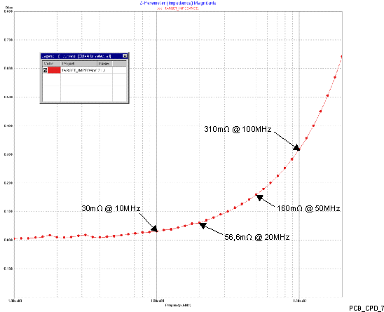
Impedance target for key frequency of interest between Processor input power balls and PMIC’s SMPS output power balls should not exceed 57mΩ at 20MHz.
Table 8-7 Example PCB vdd_mpu PI Analysis Summary
| Parameter | Recommendation | Example PCB |
|---|---|---|
| Processor OPP | High | |
| Clocking Rate | 1.5 GHz | |
| Voltage Level | 1.22V | 1.22V |
| Max Current Draw | 5.12 A | 5.12 A |
| Max Effective Resistance: Power Inductor Segment Total Reff | 10mΩ | 9.0mΩ |
| Max Loop Inductance | 2.0nH | 1.0 – 1.4nH |
| Impedance Target | 57mΩ F<20Mhz | 57mΩ F<20Mhz |
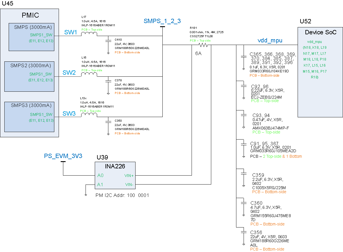
Figure 8-21, Figure 8-22, Figure 8-23, and Figure 8-24 show a PCB layout example and the resulting PI analysis results.
 Figure 8-21 vdd_mpu Simplified SCH Diagram
 ![TDA2SX TDA2SG TDA2SA TDA2HG TDA2HV TDA2HF TDA2LF vdd_mpu routing [Top Layer] TDA2SX TDA2SG TDA2SA TDA2HG TDA2HV TDA2HF TDA2LF VAYU_PCB_CPD_2.gif](/ods/images/ZHCSJ34F/VAYU_PCB_CPD_2.gif) Figure 8-22 vdd_mpu routing [Top Layer]
Figure 8-22 vdd_mpu routing [Top Layer] ![TDA2SX TDA2SG TDA2SA TDA2HG TDA2HV TDA2HF TDA2LF vdd_mpu routing [Internal Power Plane #2] TDA2SX TDA2SG TDA2SA TDA2HG TDA2HV TDA2HF TDA2LF VAYU_PCB_CPD_3.gif](/ods/images/ZHCSJ34F/VAYU_PCB_CPD_3.gif) Figure 8-23 vdd_mpu routing [Internal Power Plane #2]
Figure 8-23 vdd_mpu routing [Internal Power Plane #2] ![TDA2SX TDA2SG TDA2SA TDA2HG TDA2HV TDA2HF TDA2LF vdd_mpu routing and cap placements [Bottom Layer] TDA2SX TDA2SG TDA2SA TDA2HG TDA2HV TDA2HF TDA2LF VAYU_PCB_CPD_4.gif](/ods/images/ZHCSJ34F/VAYU_PCB_CPD_4.gif) Figure 8-24 vdd_mpu routing and cap placements [Bottom Layer]
Figure 8-24 vdd_mpu routing and cap placements [Bottom Layer] Table 8-8 PCB Etch Resistance Breakdown - From PMIC Source to Device Load
| Net[from] | Component [from]: | Net[to] | Component [to]: | Etch Resistance (Ω) | % of Total Etch Resistance |
|---|---|---|---|---|---|
| SW1 | L17 | SW1 | U45 | 0,001038 | 13% |
| SW2 | L15 | SW2 | U45 | 0,000898 | 12% |
| SW3 | L13 | SW3 | U45 | 0,000861 | 11% |
| SW1 | L17 | SMPS_1_2_3 | R181 | 0,000696 | 9% |
| SW2 | L15 | SMPS_1_2_3 | R181 | 0,000541 | 7% |
| SW3 | L13 | SMPS_1_2_3 | R181 | 0,000526 | 7% |
| vdd_mpu | R181 | vdd_mpu | U52 | 0,006311 | 78% |
| vdd_mpu | R181 | vdd_mpu | U52 | 0,006311 | 81% |
| vdd_mpu | R181 | vdd_mpu | U52 | 0,006311 | 82% |
| Total Etch Resistance from SW1 = | 0,008045 | 100% | |||
| Total Etch Resistance from SW2 = | 0,00775 | 100% | |||
| Total Etch Resistance from SW3 = | 0,007698 | 100% | |||
| Max Value = | 0,008045 | ||||
Table 8-9 PCB Etch Resistance Breakdown - From Power Inductor to Device Load
| Net[from] | Component [from]: | Net[to] | Component [to]: | Etch Resistance (Ω) | % of Total Etch Resistance |
|---|---|---|---|---|---|
| SMPS_1_2_3 | L17 | SMPS_1_2_3 | R181 | 0,000696 | 10% |
| SMPS_1_2_3 | L15 | SMPS_1_2_3 | R181 | 0,000541 | 8% |
| SMPS_1_2_3 | L13 | SMPS_1_2_3 | R181 | 0,000526 | 8% |
| vdd_mpu | R181 | vdd_mpu | U52 | 0,006311 | 90% |
| vdd_mpu | R181 | vdd_mpu | U52 | 0,006311 | 92% |
| vdd_mpu | R181 | vdd_mpu | U52 | 0,006311 | 92% |
| Total Etch Resistance = | 0,007007 | 100% | |||
| Total Etch Resistance = | 0,006852 | 100% | |||
| Total Etch Resistance = | 0,006837 | 100% | |||
| Max Value = | 0,007007 | ||||
Table 8-10 PDN Effective Resistance - From PMIC Source to Device Load
| PDN Elements | PDN Effective Resistance (Ω) | % of Total Etch Resistance |
|---|---|---|
| Etch | 0,008045 | 89% |
| Inductor | 0 | 0% |
| Sense Resistor | 0,001 | 11% |
| Max PDN Effectiv Resistance from Source | 0,009045 | 100% |
IR Drop: vdd_mpu (PCB RevJan14, Sentinel PSI)
- Source Conditions: 1.22V @ 5,12A
- Recommended Reff < 10mΩ
- Reff = Total Trace Resistance + Sence Resistor = 8,04mΩ + 1mΩ = 9,04mΩ
- Voltage / IR Drop: 1,22 - 1,179 = 52,6 mV
![TDA2SX TDA2SG TDA2SA TDA2HG TDA2HV TDA2HF TDA2LF vdd_mpu Voltage/IR Drop [All Layers] TDA2SX TDA2SG TDA2SA TDA2HG TDA2HV TDA2HF TDA2LF VAYU_PCB_CPD_5.gif](/ods/images/ZHCSJ34F/VAYU_PCB_CPD_5.gif) Figure 8-25 vdd_mpu Voltage/IR Drop [All Layers]
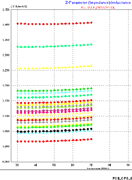
Figure 8-25 vdd_mpu Voltage/IR Drop [All Layers] Dynamic analysis of this PCB design for the MPU power domain determined the vdd_mpu decoupling capacitor loop inductance and impedance vs frequency analysis shown below. As you can see, the loop inductance values ranged from 1.0 to 1.4nH and were less than maximum 2.0nH recommended.
NOTE
Comparing loop inductances for capacitors at different distances from the processor’s input power balls shows an 18% reduction for caps placed closer. This was derived by averaging the inductances for the 3 caps with distances over 800mils (Avg LL = 1.33nH) vs the 3 caps with distances less than 600mils (Avg LL = 1.096nH).
Table 8-11 Rail - vdd_mpu
| Cap Ref Des | Model Port # | Loop Inductacne [nH] | Footprint Types | PCB Side | Distance to Ball-Field [mils] | Value [μF] | Size |
|---|---|---|---|---|---|---|---|
| C356 | 1 | 1,4 | 4vWSE | Bottom | 897 | 22 | 0603 |
| C359 | 2 | 1,26 | 4vWSE | Bottom | 855 | 2,2 | 0402 |
| C360 | 3 | 1,33 | 4vWSE | Bottom | 850 | 4,7 | 0402 |
| C365 | 4 | 1,14 | 4vWSE | Bottom | 817 | 0,1 | 0201 |
| C366 | 5 | 1,13 | 4vWSE | Bottom | 755 | 0,1 | 0201 |
| C367 | 6 | 1,07 | 4vWSE | Bottom | 758 | 1 | 0201 |
| C368 | 7 | 1,12 | 4vWSE | Bottom | 811 | 0,1 | 0201 |
| C369 | 8 | 1,06 | 4vWSE | Bottom | 690 | 0,1 | 0201 |
| C370 | 9 | 1,12 | 4vWSE | Bottom | 680 | 0,1 | 0201 |
| C384 | 10 | 1,04 | 4vWSE | Bottom | 686 | 0,1 | 0201 |
| C385 | 11 | 1,07 | 4vWSE | Top | 686 | 0,1 | 0201 |
| C387 | 12 | 1,16 | 4vWSE | Top | 755 | 0,1 | 0201 |
| C389 | 13 | 1,18 | 4vWSE | Top | 693 | 0,1 | 0201 |
| C391 | 14 | 1,14 | 4vWSE | Bottom | 693 | 0,1 | 0201 |
| C392 | 15 | 1,18 | 4vWSE | Bottom | 542 | 0,1 | 0201 |
| C396 | 16 | 1,11 | 4vWSE | Bottom | 745 | 0,1 | 0201 |
| C91 | 17 | 1,1 | 4vWSE | Bottom | 515 | 1 | 0201 |
| C92 | 18 | 1,09 | 4vWSE | Bottom | 622 | 0,22 | 0201 |
| C93 | 19 | 1,01 | 4vWSE | Bottom | 504 | 0,47 | 0201 |
| C94 | 20 | 1,13 | 4vWSE | Bottom | 604 | 0,47 | 0201 |
| C95 | 21 | 1,04 | 4vWSE | Bottom | 612 | 1 | 0201 |
| C96 | 22 | 1,08 | 4vWSE | Top | 612 | 0,22 | 0201 |
Loop Inductance range: 1,01 - 1,40 nH
 Figure 8-26 vdd_mpu Decoupling Cap Loop Inductances
 Figure 8-27 shows vdd_mpu Impedance vs Frequency characteristics.
 Figure 8-27 vdd_mpu Impedance vs Frequency